It is likely that - almost no matter where you were - you were aware that a solar eclipse occurred in the Western U.S. in the middle of October, 2023. Wanting to go somewhere away from the crowds - but along the middle of the eclipse path - we went to an area in remote west-central Utah in the little-known Conger Mountains.
Clint, KA7OEI operating CW in K-6085 with Conger mountain and the JPC-7 loaded dipole in the background. Click on the image for a larger version.
Having lived in Utah most of my life, I hadn't even heard of this mountain range even through I knew of the several (nearly as obscure) ranges surrounding it. This range - which is pretty low altitude compared to many nearby - peaks out at only about 8069 feet (2460 Meters) ASL and is roughly 20 miles (32km) long. With no incorporated communities or paved roads anywhere nearby we were, in fact, alone during the eclipse, never seeing any other sign of civilization: Even at night it was difficult to spot the glow of cities on the horizon.
For the eclipse we set up on BLM (Bureau of Land Management) land which is public: As long as we didn't make a mess, we were free to be there - in the same place - for up to 14 days, far more than the three days that we planned. Our location turned out to be very nice for both camping and our other intended purposes: It was a flat area which lent itself to setting up several antennas for an (Amateur) radio propagation experiment, it was located south and west of the main part of the weather front that threatened clouds, and its excellent dark skies and seeing conditions were amenable to setting up and using my old 8" Celestron "Orange tube" C-8 reflector telescope.
(Discussion of the amateur radio operations during the eclipse are a part of another series of blog entries - the first of which is here: Multi-band transmitter and monitoring system for Eclipse monitoring (Part 1) - LINK)
Activating K-6085
Just a few miles away, however, was Conger Mountain itself - invisible to us at our camp site owing to a local ridge - surrounded by the Conger Mountain BLM Wilderness Area, which happens to be POTA (Parks On The Air) entity K-6085 - and it had never been activated before. Owing to the obscurity and relative remoteness of this location, this is not surprising.
Even though the border of the wilderness area was less than a mile away from camp as a crow files, the maze of roads - which generally follow drainages - meant that it was several miles driving distance, down one canyon and up another: I'd spotted the sign for this area on the first day as we our group had split apart, looking for good camping spots, keeping in touch via radio.
Just a few weeks prior to this event I spent a week in the Needles District of Canyonlands National Park where I could grab a few hours of POTA operation on most days, racking up hundreds of SSB and CW contacts - the majority of being the latter mode (you can read about that activation HERE). Since I had already "figured it out" I was itching to spend some time activating this "new" entity and operating CW. Among those others in our group - all of which but one are also amateur radio operators - was Bret, KG7RDR - who was also game for this and his plan was to operate SSB at the same time, on a different band. As we had satellite Internet at camp (via Starlink) we were able to schedule our operation on the POTA web site an hour or so before we were to begin operation.
In the late afternoon of the day of the eclipse both Bret and I wandered over, placing our stations just beyond the signs designating the wilderness study area (we read the signs - and previously, the BLM web site - to make sure that there weren't restrictions against what we were about to do: There weren't.) and several hundred feet apart to minimize the probability of QRM. While Bret set up a vertical, non-resonant end-fed wire fed with a 9:1 balun suspended from a pole anchored to a Juniper, I was content using my JPC-7 loaded dipole antenna on a 10' tall studio light stand/tripod.
Bret, KG7RDR, operating 17 Meter SSB - the mast and vertical wire antenna visible in the distance. Click on the image for a larger version.
Initially, I called CQ on 30 meters but I got no takers: The band seemed to be "open", but the cluster of people sending out just their callsign near the bottom of the band indicated to me that attention was being paid to a rare station, instead. QSYing up to 20 meters I called CQ a few times before being spotted and reported by the Reverse Beacon Network (RBN) and being pounced upon by a cacophony of stations calling me.
Meanwhile, Bret cast his lot on 17 meters and was having a bit more difficulty getting stations - likely due in part to the less-energetic nature of 17 meter propagation at that instant, but also due to the fact that unlike CW POTA operation where you can be automatically detected and "spotted" on the POTA web site, SSB requires that someone spot your signal for you if you can't do it yourself: Since we had no phone or Internet coverage at this site, he had to rely on someone else to do this for him. Despite these challenges, he was able to make several dozen contacts.
Back at my station I was kept pretty busy most of the time, rarely needing to call CQ - except, perhaps, to refresh the spotting on the RBN and to do a legal ID every 10 minutes - all the while making good use of the narrow CW filter on my radio.
As it turned out, our choice to wait until the late afternoon to operate meant that our activity spanned two UTC days: We started operating at the end of October 14 and finished after the beginning of October 15th meaning that with a single sitting, each of us accomplished two activations over the course of about 2.5 hours. All in all I made 85 CW contacts (66 of which were made on the 14th) while Bret made a total of 33 phone contacts.
We finally called it quits at about the time the sun set behind a local ridge: It had been very cool during the day and the disappearance of the sun caused it to get cold very quickly. Anyway, by that time we were getting hungry so we returned to our base camp.
Back at camp - my brother and Bret sitting around the fake fire in the cold, autumn evening after dinner. Click on the image for a larger version.
My station
My gear was the same as that used a few weeks prior when I operated from Canyonlands National Park (K-0010): An old Yaesu FT-100 equipped with a Collins mechanical CW filter feeding a JPC-7 loaded dipole, powered from a 100 amp-hour Lithium-Iron-Phosphate battery. This power source allowed me to run a fair bit of power (I set it to 70 watts) to give others the best-possible chance of hearing me.
As you would expect, there was absolutely no man-made noise detectable from this location as any noise that we would have heard would have been generated by gear that we brought, ourselves. I placed the antenna about 25' (8 meters) away from my operating position, using a length of RG-8X as the feedline, placing it far enough away to eliminate any possibility of RFI - not that I've ever had a problem with this antenna/radio combination.
I did have one mishap during this operation. Soon after setting up the antenna, I needed to re-route the cable which was laying on the ground, among the dirt and rocks, and I instinctively gave it a "flip" to try to get it to move rather than trying to drag it. The first couple of "flips" worked OK, but every time I did so the cable at the far end was dragged toward me: Initially, the coax was dropping parallel with the mast, but after a couple flips it was at an angle, pulling with a horizontal vector on the antenna and the final flip caused the tripod and antenna to topple, the entire assembly crashing to the ground before I could run over and catch it.
The result of this was minor carnage in that only the (fragile!) telescoping rods were mangled. At first I thought that this would put an end to my operation, but I remembered that I also had my JPC-12 vertical with me which uses the same telescoping rods - and I had a spare rod with that antenna as well. Upon a bit of inspection I realized, however, that I could push an inch or so of the bent telescoping rod back in and make it work OK for the time-being and I did so, knowing that this would be the last time that I could use them.
The rest of the operating was without incident, but this experience caused me to resolve to do several things:
Order more telescoping rods. These cost about $8 each, so I later got plenty of spares to keep with the antenna.
Do a better job of ballasting the tripod. I actually had a "ballast bag" with me for this very purpose, but since our location was completely windless, I wasn't worried about it blowing over.
If I need to re-orient the coax cable, I need to walk over to the antenna and carefully do so rather than trying to "flip" it get it to comply with my wishes.
* * *
Epilogue: I later checked the Reverse Beacon Network to see if I was actually getting out during my initial attempt to operate on 30 meters: I was, having been copied over much of the Continental U.S. with reasonably good signals. I guess that everyone there was more interested in the DX!
P.S. I really need to take more pictures during these operations!
In part 1 (linked above) we discussed a simple two-element "TDOA" (Time Difference Of Arrival) system for determining the bearing to a transmitter. This method takes advantage of the fact that - under normal conditions - one can presume the incoming signal to be a wave "front", which is to say like ripples in water from a very distant source, they "sweep" over the receiver in lines that are at a right-angle to the direction from the transmitter. Note that in this discussion, most of the emphasis will be placed on how it is done in the analog domain with switching antennas as this can help provide a clearer picture of what is going on.
Why this works
If we are using a two-antenna array, we can divine a difference between the arrival time of the two antennas as this drawing - stolen from part 1 of this article - illustrates:
Figure 1:
A diagram showing how the "TDOA" system works. Click on the image for a larger version.
As illustrated in the top portion of the above illustration, the wave front "hits" the two elements at exactly the same time so, in theory, there is no difference between the signal from each of these elements. In the bottom portion of the illustration, we can see that the wave front will hit the left-most element first and the RF will be out of phase at the second element (e.g. one element will "see" a the positive portion of the wave and the other will see the negative portion of the wave).
If we constrain ourselves with having just ONE receiver to use, you might ask yourself how one might use the signal from two antennas? The answer is that one switches between the two antennas electronically - typically with diodes. If the two signals are identical in their time of arrival - and the length of coaxial cable between the antenna and when one switches "perfectly" between the two antennas and there is no disturbance in the received signal, we know that the signal is likely to be broadside of our two-antenna array.
If the signal is NOT broadside to the the array, there will be a "glitch" in the waveform coming out of our receiver when we switch our antenna. Because we are using an FM receiver - which detects modulation by observing the frequency change caused by audio modulation - we can also detect that "glitch". To understand how this works, consider the following:
Recall the "Doppler Effect" (Wikipedia article - link) where the pitch of the horn of a car increases from its original when it is moving toward the observer - and it is lower in pitch when it moves away from the observer: It is only at the instant that the car is closest to the observer that the pitch heard is the actual pitch of the horn.
Now, consider this same thing when we look at the lower diagram of Figure 1. If we switch from the left-hand antenna to the right-hand antenna, we have effectively moved away from the transmitter and for an instant the frequency of the received signal was lower because - from the point of the receiver on the end of the coax cable - the antenna moved away from the transmitter. Because changes in frequency going up and down cause the voltage coming out of the receiver to go up and down by the same amount, we will get a brief "glitch" from having changed the frequency for a brief instant when our antenna "moved".
If we then switch back from the right-hand antenna to the left-hand antenna, we have suddenly moved it closer to the transmitter and, again, we shift the frequency - but in the opposite direction, and the glitch we get in the receiver is opposite as well.
We can see the glitching of this signal in the following photo, also stolen from "Part 1" of this article:
Figure 2: Example of the "glitches" seen on the audio of a receiver connected to a TDOA system that switches antennas.
The photo in Figure 2 is that of an oscilloscope trace of the audio output of the FM receiver connected to it and in it, we can see a positive-going "glitch" when we switch from one antenna to the other, and a negative-going glitch when we switch back again.
If we have a simple circuit that is switching the antennas back-and-forth - and it "knows" when this switch happens, we can determine several things:
When the two antennas are broadside to the transmitter. If we have the situation depicted in the top drawing of Figure 1, both antennas are equidistant and there will be NO glitches detected.
When antenna "A" is closer to the transmitter. If we arbitrarily assign one of the antennas as "A" and the other as "B", we can see - by way of our "thought experiment" above - that if antenna "A" is closer to the transmitter than "B", our frequency will go DOWN for an instant when we switch from "A" to "B" - and vice-versa when it switches back. Let us say that this produces the pattern of "glitches" that we seen in Figure 2.
When antenna "B" is closer to the transmitter. If we take the above situation and rotate our two-antenna array around 180 degrees, antenna "B" will be closer to the transmitter than "A" and when our switch from "A" to "B" happens, our frequency will go UP for an instant when it does so - and vice-versa. In that case, our oscilloscope will show the glitches depicted in Figure 2 upside-down.
In other words, by looking at the polarity of the glitches from our receiver, we can tell if the transmitter is to our left or to our right. We can also infer a little bit about how far to the left or right our transmitter is by looking at the amplitude of the glitches: If the signal is off the side of the antenna as depicted in the lower part of Figure 1, the glitches will be at the strongest - and the amplitude of the glitches will diminish as we get closer to having the two elements parallel as depicted in the top part of Figure 1.
There is an obvious limitation to this:Unless we sweep the antenna back and forth, allwe can do is tell if the antenna is to our left or right.
Walking about with an antenna like this it is easy to sweep back and forth and with some practice, one can infer whether the the transmitter is to the left or right and in front or behind - but if you have a fixed antenna array (one that is not moving) or if you are in a vehicle where their orientation is fixed with respect to the direction of travel, this becomes inconvenient as you cannot tell if it is in front or behind.
Adding more antennas
Suppose that we want to know both "left and right" and "front and back" at the same time - and in that case, you would be correct if you presumed that you were to be able to do this by adding one more antenna and - and then did some switching between them. Consider the case in Figure 3, below:
Figure 3: A 3-antenna vertical array, with elements A, B and C. A right-angle is formed between antennas "A" and "B" and "A" and "C". Also see Figure #4. Click on the image for a larger version.
In Figure 3 and 4 we have three vertical antennas - separated by less than 1/4 wavelength at the frequency of interest 1 and we also have two transmitters located 90 degrees apart from each other. Note that these antennas are laid out in a "three-sided square" - that is, if you were to draw lines between "A" and "B" and "A" and "C" they would form a precise right angle.
We know already from our example in Figure 1that if we are receiving Transmitter #1 that we will get our "glitch" if we switch between antenna "A" and "B" - but since antennas "A" and "C" are the same distance from Transmitter #1, we will get NO glitch.
Similarly, if we are listening to Transmitter #2, if we switch between antenna "A" and "C", we will get a glitch as "C" is closer to the transmitter than "A" - but since antennas "A" and "B" are the same distance, we would get not glitch.
From this example we can see that if we have three antennas, we can switch them alternately to resolve our "Left/Right" and "Front/Back" ambiguity at all times. For example, let us consider what happens in the presence of Transmitter #2:
Switch from antenna "A" to antenna "B": The antennas are equidistant from Transmitter #2, so there is no glitch.
Switch from antenna "A" to antenna "C": We get a glitch in our received audio when we do this because antenna "C" is closer to Transmitter #2 than antenna "A". Furthermore, we can tell by the polarity of the glitch that antenna "C" is closer to the transmitter.
Let us now presume that our array in Figure 3 and 4 was atop a vehicle and the front of the vehicle was pointed toward the left - toward Transmitter #1: With just the above information we would know that this transmitter was located precisely to our right - and that if we wanted to drive toward it, we would need to make a right turn.
Figure 4: A 3-antenna vertical array, with elements A, B and
C as viewed from the top. Click on the image for a larger version.
Bearings in between the antennas
What if there a third transmitter (Transmitter #3 in Figure 4) located halfway between Transmitter #1 and Transmitter #2 and we were still in our car pointed at Transmitter #1? You would be correct in presuming that:
Switching between Antenna "A" and "B" would indicate that the unknown transmitter would be to the front of the car.
Switching between Antenna "A" and "C" would indicate that the unknown transmitter would be to the right of the car.
We get "glitches" when switching between either pairs of antennas (A/B and A/C) - but these "glitches" are at lower amplitude than if the transmitter were in the direction of Transmitter #1 or Transmitter #2.
Could it be that if we measured the relative amplitude and polarity of the glitches we get from switching the two pairs of antennas (A/B and A/C) that we could infer something about the bearing of the signal?
The answer is YES.
By using simple trigonometry we can figure out - by comparing the amplitudes of the glitches and noting their relative polarity - the bearing of the transmitter with respect to the antenna array - and the specific thing we need is the inverse function "ArcTangent".
If you set your "Wayback" machine to High School, you will remember that you could plot a point on a piece of X/Y graph paper and relative to the origin, use the ratio of the X/Y values to determine the angle of a line drawn between that point and the origin. As it turns out, there is a function in many computer languages that is useful in this case - namely the "atan2()" function in which we put our "x" and "y" values.
Figure 5: Depiction of the "atan2" function and how to get the angle, θ. This diagram is modified from the Wikipedia "atan2" article - link. Click on the image for a larger version.
Let us consider the drawing in Figure 5. If you remember much of your high-school math, you'll remember that if straight-up is zero degrees and the right-pointing arrow is 90 degrees that the "mid-point" between the two would naturally be 45 degrees.
What you might also remember is that if you were drop a line between the dot marked as (x,y) in Figure 5 and the "x" axis - and draw another line between it and the "y" axis - those lines would be the same length.
By extension, you can see that if you know the "x" and "y" coordinates of the dot depicted in Figure 5 - and "x" and/or "y" can be either positive or negative - you can represent any angle.
Referring back to Figure 2, recall that you will get a "glitch" when you switch antennas that are at different distances from the transmitter - and further recall that in Figures 3 and 4 that you can use the switching between antennas "A" and "B" to determine if the transmitter is in front or behind the car - and "A" and "C" to determine if it is to the left or right of the car.
If we presume that the "y" axis (up/down) is front/back of the car and the "x" axis is right/left, we can see that if we have an equal amount of "glitching" from the A/B switch ("y" axis) and the A/C switch ("x" axis) - and both of these glitches go positive - we would then know that the transmitter was 45 degrees to the right of straight ahead.
Similarly, if we were to note that our "A/B" ("y" axis) glitch was very slightly negative - indicating that the signal was behind and and that our "A/C" glitch was strongly negative indicating that it was far to our left: This condition is depicted with the vector terminating in point "A" in Figure 5 to show that the transmitter was, in fact, to the left and just behind us - perhaps at an angle of about 260 degrees.
Using 4 antennas
The use of three antennas isn't common - particularly with an "L" (right-angle) arrangement - but one could do that. What is more common is to arrange four antennas in a square and "rotate" them using diode switches with one antenna being active at a given instant - and having more antennas and more switching between antennas to create our glitches gives us more data to work with which can only help reduce the uncertainty of the bearing. Consider the diagram of Figure 6.
Figure 6: A four antenna arrangement. Click on the image for a larger version.
In this arrangement we have four antennas arranged in a perfect square - and this time we are going to switch them in the following pattern:
A->B->C->D->A
Now let us suppose that we are receiving Transmitter "A" - so we would get the following "glitch" patterns on our receiver:
A->B: Positive glitch (A is closer to TX #1 than B so the the source is seen to move farther away)
B->C: No glitch (B and C are the same distance from TX #1)
C->D: Negative glitch (D is closer to TX #1 than C so the source is seen to move closer)
D->A: No glitch (A and B are the same distance from TX #1)
As expected, going from "A" to "B" results in a glitch that we'll call "positive" as antenna "B" is farther away from the transmitter than "A" - but when we "rotate" to the other side and switch from "C" to "D" - because we are going toan antenna that is closer, the glitch will have the opposite polarity as the one we got when we switched from "A" to "B" - but both glitches will have the same amplitude.
Since antenna pairs B/C and A/D are the same distance from the transmitter we will get no glitch when we switch between those antennas.
As you can see from the above operation, every time we make one "rotation", we'll get four glitches - but they will be in equal and opposite pairs - which is to say the A->B and the C->D are one pair with opposite polarity and B->C and D->A are the other pair with opposite polarity. If we take the measured voltage of these pairs of glitches and subtract each set, we will end up with vectors that we can throw into our "atan2" function and get a bearing - and what's more, since we are getting the same information twice(the equal-and-opposite pairs) this serves to increase the effective amplitude of the glitch overall to help make it stand out better from modulation and noise that may be on the received signal.
Similarly, if we were receiving a signal from Transmitter #3 (in Figure 6) we could see that being at a 45 degree angle, each of our four glitches would have the same strength but differing polarities - with the vector pointing in that direction. What's more, the magnitude of those glitches will be a bit lower than our example with Transmitter #1, above: Since Transmitter #3 is shifted 45 degrees, this means that the apparent distance between any antenna switch will be about 71% as great as it would have been had it been Transmitter #1 or #2. If you recognized that 71% - or 0.707 is the sine (or cosine) of 45 degrees, you would be exactly right!
A typical four-antenna ARDF unit will "spin" the antenna at anywhere between 300 and 1000 RPM - the lower frequencies being preferable as it and their harmonics are better-contained within the 3 kHz voice bandwidth of a typical communications-type FM receiver.
Figure 7: Montreal "Dopplr 3" with compass rose, digital bearing indication and adjustable switched- capacitor band-pass filter running "alternate" firmware (see KA7OEI link below). Click on the image for a larger version.
Improving performance - filtering
As can be seen in the oscillogram of Figure 2, the switching glitches are of pretty low amplitude - and they are quite narrow meaning that they are easily overwhelmed by incidental audio and - in the case of weaker signals - noise. One way to deal with this is to use a very narrow audio band-pass filter - typically something on the order of a few Hz to a few 10s of Hz wide.
In the analog world this is typically obtained using a switched-capacitor - the description of which would be worthy of another article - but it has the advantage of its center frequency being set by an external clock signal: If the same clock signal is used for both the filter and to "spin" the antenna, any frequency drift is automatically canceled out.
It is also possible to use a plain, analog band-pass filter using op amps, resistors and capacitors - but these can be problematic in that these components - particularly the capacitors - are prone to temperature drift which can affect the accuracy of the bearing, often requiring repeated calibration: This problem is most notable during summer or winter months when the temperature can vary quite a bit - particularly in a vehicle.
By narrowing the bandwidth significantly - to just a few Hz - it is far more likely that the energy getting through it will be only from the antenna switching and not incidental audio.
There is another aspect related to narrow-band filtering that can be useful: Indicating the quality of signal. In the discussions above, we are presuming that opposite pairs of antennas will yield equal-and-opposite "glitches" (e.g. A->B and C->D are mirror images, and B->C and D->A are also mirror images) - but in the case of multipath distortion - where the receive signal can come from different directions due to reflection and/or refraction - this may not be the case. If the above "mirroring" effect is not true, this causes changes in the amplitude of the tone from the antenna spin rate (the "switching tone") which can include the following:
The switching tone can decrease overall due to a multiplicity of random wave fronts arriving at the antenna array.If multipath is such that one or more of our antennas gets no signal - or they get a delayed bounce that "looks" like one of the other antennas, you might get a missing glitch or one that has the wrong polarity. A signal distorted in such a manner probably won't make it through our very narrow band-pass filter very well at all.
The switching tone's frequency can double if each antenna's slightly-different position is getting a different portion of a multipath-distorted wave front.If the multipath is such that every antenna as a different version of the bounced signal it may be that you don't get the "equal and opposite" glitches that you expect. Again, if our switching tone is doubled, it won't make it through the band-pass filter.
The switching tone can be heavily frequency-modulated by the rapidly-changing wave fronts. Remember that Frequency Modulation is all about the rapid phase changes of the carrier with modulation - but if you are driving through an area with a lot of reflections, this can add random phase shifts to the received signal which can cause the switching tone of our antennas' rotation to be seemingly randomized. Because the randomization will likely appear as noise, this will likely "dilute" our switching tone and there will be less of it to be able to get through our narrow band-pass filter.
If you have everoperated VHF/UHF from a moving vehicle, you have experienced all three of the above to a degree: It's likely that you have stopped at a light or a sign, only to find out that the signal to which you were listening faded out and/or got distorted - only to appear again if you moved your vehicle forward or backwards even a few inches/centimeters. Similarly, you've likely heard noise (e.g. "Picket Fencing")as you have driven through an area with a lot of clutter from buildings and/or terrain: Imagine this happening to four antennas in slightly different locations on the roof of your vehicle, each getting a signal that is distorted in its own, unique way!
Each of the above cause the switching tone in the receiver to be disrupted and with the worse disruption, less of the signal will get through the narrow filter. Of course, having a good representation of the antenna's switching tone does not automatically mean that it is going to indicate a true bearing to the transmitter as you could be receive a "clean" reflection - but you at least you can detect - and throw out - obviously "bad" information!
Improving performance - narrow sampling
In addition to - or instead of narrow-band sampling - there's another method that could be used and that is narrow sampling. Referring to Figure 2 again, you'll note that the peaks of the glitches are very narrow. While the oscillogram of Figure 2 was taken from the speaker output of the receiver, many radios intended for packet use also include a discriminator output for use with 9600 baud and VARA modes which has a more "pristine" version of this signal.
Because we can know precisely when this glitch arrives (e.g. we know when we switch the antenna - and we can determine by observation when, exactly, it will appear on the radio's output) we can do a grab the amplitude of this pulse with a very narrow window (e.g. "look" for it precisely when we expect it to arrive) and thus reject much of the audio content and noise that can interfere with our analysis.
Further discussion of this technique is beyond the scope of this article, but it is discussed in more detail here.
Improving performance - vector averaging
If you have ever used a direction-finding unit with an LED compass rose before, you'll note that in areas of multipath that the bearing seems to go all over the place - but if you look very carefully (and are NOT the one driving) you may notice something interesting: Even in areas of bad multipath, there is likely to be a statistical weight toward the true bearing rather than a completely random mess. This is a very general statement and it refers more to those instances where signals are blocked more by local ground clutter rather than a strong reflection from, say, a mountain, which may be more consistent in their "wrongness".
While the trained eye can often spot a tendency from seemingly-random bearings, one can bring math to the rescue once again. Because we are getting our signal bearings by inputting vectors into the "atan2" function, we could also sum the individual "x" and "y" vectors over time and get an average.
This works in our favor for at least two reasons:
It is unlikely that even multipath signals are entirely random. As signals bounce around from urban clutter, it is likely that there will be a significant bias in one particular direction.
Through vector averaging, the relative quality of a signal can be determined. If you get a "solid" bearing with consistently-good signals, the magnitude of the x/y vectors will be much greater than that from a "noisy" signal with a lot of variation.
In the case of #1, it is often that, while driving through a city among buildings that the bearing to a transmitter will be obfuscated by clutter - but being able to statistically reduce "noise" may help to provide a clue as to a possible bearing.
In the case of #2, being able to determine the quality of the bearing can, through experience, indicate to you whether or note you should pay attention to the information that you are getting: After all, getting a mix of good and bad information is fine as long as you know which is the bad information!
Typically one would use a slidingaverage consisting of a recent history of samples. If one uses the "vector average" method described above it is more likely that poor-quality bearings will have a lesser influence on the result.
Antenna switching isn't ideal
Up to this point we have been talking about using a single receiver with a multi-antenna array that sequentially switches individual antennas into the mix - but electronic switching of the antennas is not ideal for several reasons:
The "modulation" due to the antenna switching imparts sidebands on the received signals. Because this switching is rather abrupt, this can mean that signals 10s and 100s of kHz away can raise the receive system noise floor and decrease sensitivity.
The switching itself is quite noisy in its own right and can significantly reduce the absolute sensitivity of the receive system. For this reason, only "moderate-to-strong" signals are good candidates for this type of system.
In the presence of multipath, the switching itself can result in the signal being more highly disrupted than normal. This isn't too much of a problem since it is unlikely that one could get a valid bearing in that situation, anyway, but it can still be mitigated with filtering as described above.
If one is actively direction-finding with gear like this, it should not be the only tool in their toolbox: Having a directional antenna - like a small Yagi - and suitable receiver (one with a useful, wide-ranging signal level meter) is invaluable both for situations where the signal may be too weak to be reliably detected with a TDOA system and when you are so close to it that you may have to get out of the vehicle and walk around.
Doing this digitally
There is something to be said about the relative simplicity of an analog TDOA system: You slap the antennas on the vehicle, perform a quick calibration using a repeater or someone with a handie-talkie, and off you go. To be sure, a bit of experience is invaluable in helping you to determine when you should and should not trust the readings that you are getting - but eventually, if the signal persists, you will likely find the source of the signal.
These days there are a number of SDR (Software-Defined Radio) systems - namely the earlier Kerberos and more recent Kraken SDRs. Both of these units use multiple receivers that are synchronized from the same clock and use in-built references for calibration.
The distinct advantage of having a "receiver per antenna" is that one need not switch the antennas themselves, meaning that the noise and distortion resulting from the electronic "rotation" is eliminated. Since the antennas are not switched, a different - yet similar - approach is required to determine the bearing of the signal - but if you've made it this far, it's not unfamiliar: The use of "atan2" again: One can take the vector difference of the signal between adjacent antennas and get some phasing information - and since we have four antennas, we can, again, get two equal and opposite pairs(assuming no multipath) of bearing data.
If you have two signals from adjacent antennas - let's say "A" and "B" from Figure 6 - we already know that the phasing will be different on the signal if the antenna hits "A" first rather than "B" first and this can be used in conjunction with its opposite pair of antennas ("C" and "D") to divine one of our vectors: A similar approach can be done with the other opposite pairs - B/C and D/A.
This has the potential to give us better-quality bearings - but the same sorts of averaging and noise filtering must be done on the raw data as it has no real advantage over the analog system in areas where there is severe multipath: It boils down to how it does its filtering and signal quality assessment and, more importantly, how you, the operator, interpret the data based on experience gained from having used the system enough have become familiar with it.
As far as absolute sensitivity goes between a Kerberos/Kraken SDR and an analog unit - that's a bit of a mixed bag. Without the switching noise, the absolute sensitivity can be better, but in urban areas - and particularly if there is a strong signal within the passband of the A/D converter (which has only 8 bits) the required AGC may necessarily reduce the gain to where weaker signals disappear.
There are other possibilities when it comes to SDR-based receivers - for example, the SDRPlay RSPduo has a pair of receivers within it that can be synchronous to each other: Using one of these units with a pair of magnetic loops can be used to effect the digital version of an old-fashioned goniometer! This has the advantage of relative simplicity and can take advantage of the relatively high performance of the RSP compared to the RTL-SDR.
Finally, there exist multi-site TDOA systems where the signals are received and time-stamped with great precision: By knowing when, exactly, a signal arrives and then comparing this with the arrival time at other, similar, sites it is (theoretically) possible to determine the location of origin - a sort of "reverse GPS" system. This system has some very definite, practical limits related to dissemination of receiver time-stamping and the nature of the received signal itself and would be a topic of of a blog post by itself!
Equipment recommendations?
My "go to " ARDF unit for in-vehicle use is currently a Montreal "Dopplr 3" running modified firmware (written by me - see the link to the "KA7OEI ARDF page, below) with four rooftop antennas. Having used this unit for nearly 20 years, I'm very familiar with its operation and have used it successfully many times to find transmitters - both in for fun and for "serious" use (e.g. stuck transmitter, jammer, etc.)
This unit has the advantage of being "grab 'n' go" in that it takes only a few seconds to "boot up" and it has a very simple, intuitive compass rose display. I believe that its performance is about as good as it can possibly be with a "switched antenna" type of ARDF unit: For the most part, if a signal is audible, it will produce a bearing.
A disadvantage of this unit to some would be that it's available only in the form or a circuit board (still available from FAR circuits - link ) which means that the would-be builder must get the parts and put it together themselves.
"Pre-assembled" options for this type of unit include the MFJ-5005 which can sometimes be found on the used market and several options from the former Ramsey Electronics - along with the Dick Smith ARDF unit: Information on these units may be found on the K0OV page linked below.
Comment: Do NOT try to use ANY ARDF gear with inexpensive Chinese radios like BaoFengs. The reason for this is that owing to their "receiver on a chip" having its own DSP processor, there are variations on how long the audio is delayed with respect to when the signal arrives at the antenna and this will certainly wreck any attempt at doing anything that requires consistent timing - which is true for all systems that use multiple antennas. You will be much better off using a "conventional" (non-DSP) receiver: Radios that are decades old - particularly if they don't have any features - are often ideal as they are typically robust and can be bought inexpensively.
Another possible option is the "Kraken SDR": I have yet to use one of these units, but I'm considering doing so for evaluation and comparison - which I will report here if I am actually able to do so.
Final words
This (rambling) dissertation about TDOA direction finding hopefully provides a bit of clarity when it comes to understanding how such things work - but there are a few things common to all systems that cannot really be addressed by the method of signal processing - analog or digital:
Bearings from a single fixed location should be suspect. Unless you happen to have an antenna array atop a tall tower or mountain, expect the bearing that you obtain to be incorrect - and even if you do have it located in the clear, bogus readings are still likely.
Having multiple sources of bearings is a must. Having more than one fixed location - or better yet having one or more sources of bearings from moving vehicles is very useful in that this dramatically decreases the uncertainty.
The most important information is often just knowing the direction in which you should start driving. Expecting to be able to located a signal with a TDOA system with any reasonable accuracy is unrealistic. It is often the case that when a signal appears, the most useful piece of information is simply knowing in which direction - to the nearest 90 degrees - that one should start looking.
The experience of the operator is paramount. No matter which system you are using, its utility is greatly improved with familiarity of its features - and most importantly, its limitations. In the real world, locating a signal source is often an exercise in frustration as it is often intermittent and variable and complicated by geography. No-one should reasonably expect to simply purchase/build such a device and have it sit on the shelf until the need arises - and then learn how to use it!
* * *
Footnote:
On systems like this where one switches between (or uses) multiple antennas - it is necessary that adjacently-compared antennas be less than a quarter wave apart at the highest operational frequency. While it is possible to get better resolution by increasing the spacing between antennas, the directional response will have multiple lobes meaning that there can be an uncertainty as to which "lobe" is being detected.
Having more than 1/4 wavelength spacing can be useful if you have means of resolving such ambiguities. Spacing antennas closer than 1/4 wavelength can work, but the phase difference also decreases meaning that differences between antennas reduces making detection of bearing more difficult and increasingly susceptible to incidental signal modulation and the uncertainty that those factors imply. From a purely practical stand point, the roof of a typical vehicle is only large enough for about 1/4 wavelength spacing on 2 meters, anyway.
It should not have escaped your attention - at least if you live in North America - there there have been/will be two significant solar eclipses occurring in recent/near times: One that occurred on October 14, 2023 and another eclipse that will happen during April, 2024. The path of "totality" of the October eclipse happened to pass through Utah (where I live) so it is no surprise that I went out of my way to see it - just as I did back in 2012: You can read my blog entry about that here.
Figure 1: The eclipse in progress - a few minutes before "annularity". (Photo by C. L. Turner)
I will shortly produce a blog entry related to my activities around the October 14, 2023 eclipse as well.
The October eclipse was of the "annular" type meaning that the moon is near-ish apogee meaning that the subtended angle of its disk is insufficient to completely block the sun owing to the moon's greater-than-average distance from Earth: Unlike a solar eclipse, there is no time during the eclipse where it is safe to look at the sun/moon directly, without eye protection.
The sun will be mostly blocked, however, meaning that those in the path of "totality" experienced a rather eerie local twilight with shadows casting images of the solar disk: Around the periphery of the moon it was be possible to make out the outline of lunar mountains - and those unfortunate to stare at the sun during this time will receive a ring-shaped burn to their retina.
From the aspect of a radio amateur, however, the effects of a total and annular solar eclipse are largely identical: The diminution of the "D" layer and partial recombination of the "F" layers of the ionosphere causing what are essentially nighttime propagation conditions during the daytime - geographically limited to those areas under the lunar shadow.
In an effort to help study these sort of effects - and to (hopefully) better-understand the propagation effects, a number of amateurs went (and are) going out into the field - in or near the path of "totality" - and setting up simultaneous, multi-band transmitters.
Producing usable data
Having "Eclipse QSO Parties" where amateur radio operators make contacts during the eclipse likely goes back nearly a century - the rarity of a solar eclipse making the event even more enigmatic. In more recent years amateurs have been involved in "citizen science" where they make observations by monitoring signals - or facilitate the making of observations by transmitting them - and this happened during the October eclipse and should also happen during the April event as well.
While doing this sort of thing is just plain "fun", a subset of this group is of the metrological sort (that's "metrology", no "meteorology"!) and endeavor to impart on their transmissions - and observations of received signals - additional constraints that are intended to make this data useful in a scientific sense - specifically:
Stable transmit frequencies. During the event, the perturbations of the ionosphere will impart on propagated signals Doppler shift and spread: Being able to measure this with accuracy and precision (which are NOT the same thing!) adds another layer of extractable information to the observations.
Stable receivers. As with the transmitters, having a stable receiver is imperative to allow accurate measurement of the Doppler shift and spread. Additionally, being able to monitor the amplitude of a received signal can provide clues as to the nature of the changing conditions.
Monitoring/transmitting at multiple frequencies. As the ionospheric conditions change, its effects at different frequencies also changes. In general, the loss of ionization (caused by darkness) reduces propagation at higher frequencies (e.g. >10 MHz) and with lessened "D" layer absorption lower frequencies (<10 MHz) the propagation at those frequencies is enhanced. With the different effects at different frequencies, being able to simultaneously monitor multiple signals across the HF spectrum can provide additional insight as to the effects.
To this end, the transmission and monitoring of signals by this informal group have established the following:
GPS-referenced transmitters. The transmitters will be "locked" to GPS-referenced oscillators or atomic standards to keep the transmitted frequencies both stable, accurate - and known to within milliHertz.
GPS referenced receivers. As with the transmitters, the receivers will also be GPS-referenced or atomic-referenced to provide milliHertz accuracy and stability.
With this level of accuracy and precision the frequency uncertainties related to the receiver and transmitter can be removed from the Doppler data. For generation of stable frequencies, a "GPS Disciplined Oscillator" is often used - but very good Rubidium-based references are also available, although unlike a GPS-based reference, the time-of-day cannot be obtained from them.
Why this is important:
Not to demean previous efforts in monitoring propagation - including that which occurs during an eclipse - but unless appropriate measures are taken, their contribution to "real" scientific analysis can be unwittingly diminished. Here are a few points to consider:
Receiver frequency stability. One aspect of propagation on HF is that the signal paths between the receiver and transmitter change as the ionosphere itself changes. These changes can be on the order of Hertz in some cases, but these changes are often measured in 10s of milliHertz. Very few receivers have that sort of stability and the drift of such a receiver can make detection of these Doppler shifts impossible.
Signal amplitude measurement. HF signals change in amplitude constantly - and this can tell us something about the path. Pretty much all modern receivers have some form of AGC (Automatic Gain Control) whose job it is to make sure that the speaker output is constant. If you are trying to infer signal strength, however, making a recording with AGC active renders meaningful measurements of signal strength pretty much impossible. Not often considered is the fact that such changes in propagation also affect the background noise - which is also important to be able to measure - and this, too, is impossible with AGC active.
Time-stamping recordings. Knowing when a recording starts and stops with precision allows correlation with other's efforts. Fortunately this is likely the easiest aspect to manage as a computer with an accurate clock can automatically do so (provided that one takes care to preserve the time stamps of the file, or has file names that contain such information) - and it is particularly easy if one happens to be recording a time station like WWV, WWVH, WWVB or CHU.
In other words, the act of "holding a microphone up to a speaker" or simply recording the output of a receiver to a .wav file with little/no additional context makes for a curious keepsake, but it makes the challenge of gleaning useful data from it more difficult.
One of our challenges as "citizen scientists" is to make the data as useful as possible to us and others - and this task has been made far easier with inexpensive and very good hardware than it ever has been - provided we take care to do so. What follows in this article - and subsequent parts - are my reflections on some possible ways to do this: These are certainly not the only ways - or even the best ways - and even those considerations will change over time as more/different resources and gear become available to the average citizen scientist.
* * *
How this is done - Receiver:
The frequency stability and accuracy of MOST amateur transceivers is nowhere near good enough to provide usable observations of Doppler shift on such signals - even if the transceiver is equipped with a TCXO or other high-stability oscillator: Of the few radios that can do this "out of the box" are some of the Flex transceivers equipped with a GPS disciplined oscillator.
To a certain degree, an out-of-the-box KiwiSDR can do this if properly set-up: With a good, reliable GPS signals and when placed within a temperature-stable environment (e.g. temperature change of 1 degree C or so during the time of the observation) they can be stable enough to provide useful data - but there is no guarantee of such.
To remove such uncertainty a GPS-based frequency reference is often applied to the KiwiSDR - often in the form of the Leo Bodnar GPS reference, producing a frequency of precisely 66.660 MHz. This combination produces both stable and accurate results. Unfortunately, if you don't already have a KiwiSDR, you probably aren't going to get one as the original version was discontinued in 2022: A "KiwiSDR 2" is in the works, but there' no guarantee that it will make it into production, let alone be available in time for the April, 2024 eclipse.
Figure 2: The RX-888 (Mk2) - a simple and relatively inexpensive box that is capable of "inhaling" all of HF at once. Click on the image for a larger version.
The RX-888 (Mk2)
A suitable work-around has been found to be the RX-888 (Mk2) - a simple direct-sampling SDR - available for about $160 shipped (if you look around). This device has the capability of accepting an external 27 MHz clock (if you add an external cable/connector to the internal U.FL connector provided for this purpose) in which it can become as stable and accurate as the external reference.
This SDR - unlike the KiwiSDR, the Red Pitaya and others - has no onboard processing capability as it is simply an analog-to-digital coupled with a USB3 interface so it takes a fairly powerful computer and special processing software to be able to handle a full-spectrum acquisition of HF frequencies.
Software that is particularly well-suited to this task is KA9Q-Radio(link). Using the "overlap and save" technique, it is extraordinarily efficient in processing the 65 Megasamples-per-second of data needed to "inhale" the entire HF spectrum. This software is efficient enough that a modest quad-core Intel i5 or i7 is more than up to the task - and such PCs can be had for well under $200 on the used market.
KA9Q-Radio can produce hundreds of simultaneous virtual receivers of arbitrary modes and bandwidths which means that one such virtual receiver can be produced for each WSPR frequency band: Similar virtual receivers could be established for FT-8, FT-4, WWV/H and CHU frequencies. The outputs of these receivers - which could be a simple, single-channel stream or a pair of audio in I/Q configuration - can be recorded for later analysis and/or sent to another program (such as the WSJT-X suite) for analysis.
Additionally, using the WSPRDaemon software, the multi-frequency capability of KA9Q-Radio can be further-leveraged to produce not only decodes of WSPR and FST4W data, but also make rotating, archival I/Q recordings around the WSPR frequency segments - or any other frequency segments (such as WWV, CHU, Mediumwave or Shortwave broadcast, etc.) that you wish.
Comment: I have written about the RX-888 in previous blog posts:
Improving the thermal management of the RX-888 (Mk 2) - link
Measuring signal dynamics of the RX-888 (Mk 2) - link
Full-Spectrum recording
Yet another capability possible with the RX-888 (Mk2) is the ability to make a "full spectrum" recording - that is, write the full sample rate (typically 64.8 Msps) to a storage device. The result are files of about 7.7 gigabytes per minute of recording that contain everything that was received by the RX-888, with the same frequency accuracy and precision as the GPS reference used to clock the sample rate of the '888.
What this means is that there is the potential that these recordings can be analyzed later to further divine aspects of the propagation changes that occurred during, before and after the eclipse - especially by observing signals or aspects of the RF environment itself that one may not have initially thought to consider: This also can allow the monitoring of the overall background noise across the HF spectrum to see what changes during the eclipse, potentially filling in details that might have been missed on the narrowband recordings.
Because such a recording contains the recordings of time stations (WWV, WWVH, CHU and even WWVB) it may be possible to divine changes in propagation delay between those transmit sites and the receive sites. If a similar GPS-based signal is injected locally, this, too, can form another data point - not only for the purposes of comparison of off-air signals, but also to help synchronize and validate the recording itself.
By observing such a local signal it would be possible to time the recording to within a few 10s of nanoseconds of GPS time - and it would also be practical to determine if the recording itself was "damaged" in some way (e.g. missed samples from the receiver): Even if a recording is "flawed" in some way, knowing the precise location an duration of the missing data allows this to be taken into account and to a large extent, permit the data "around" it to still be useful.
Actually doing it:
Up to this point there has been a lot of "it's possible to" and "we have the capability of" mentioned - but pretty much everything mentioned so far was used during the October, 2023 eclipse. To a degree, this eclipse is considered to be a rehearsal for the April 2024 event in that we would be using the same techniques - refined, of course, based on our experiences.
While this blog will mostly refer to my efforts (because I was there!) there were a number of similarly-equipped parties out in the fields and at home/fixed stations transmitting and receiving and it is the cumulative effort - and especially the discussions of what worked and what did not - that will be valuable in preparation for the April event. Not to be overlooked, this also gives us valuable experience with propagation monitoring overall - an ongoing effort using WSPRDaemon - where we have been looking for/using other hardware/software to augment/improve our capabilities.
In Part 2 I'll talk about the receive hardware and techniques in more detail.
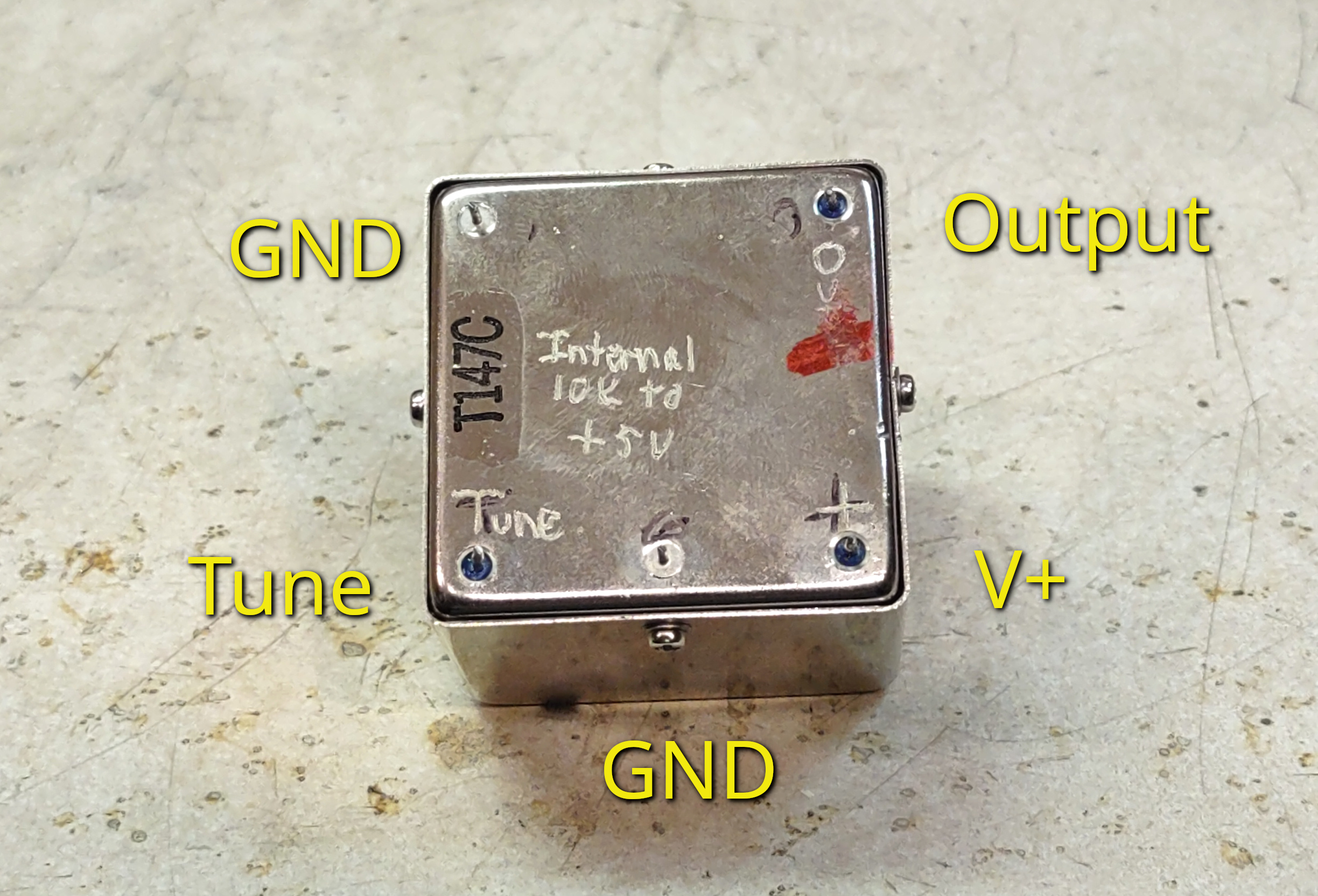
As a sort of follow-up to the previous posting about the RX-888 (Mk2) I decided to make some measurements to help characterize the gain and attenuation settings.
The RX-888 (Mk2) has two mechanisms for adjusting gain and attenuation:
The PE4312 attenuator. This is (more or less) right at the HF antenna input and it can be adjusted to provide up to 31.5dB of attenuation in 0.5dB steps.
The AD8370 PGA. This PGA (Programmable Gain Amplifier) can be adjusted to provide a "gain" from -11dB to about 34dB.
Note:
While this blog posting has specific numbers related to the RX-888 (Mk2), its general principles apply to ALL receivers - particularly those operating as "Direct Sampling" HF receivers. A few examples of other receivers in this category include the KiwiSDR and Red Pitaya - to name but two.
Other article RX-888 articles:
RX-888 Thermal issues: I recently posted another article about the RX-888 (Mk2) discussing the thermal properties of its mechanical construction - and ways to improve it to maximize reliability and durability. You can find that article here: Improving the thermal management of the RX-888 (Mk2) - link.
Using an external clock with the RX-888: The 27 MHz external clock input to the RX-888 is both fragile and fickle. To learn a bit more about how to reliably clock an RX-888 from an external source, read THIS article.
* * * * *
Taking measurements
To ascertain the signal path properties of an RX-888 (Mk2) I set its sample rate to 64 Msps and using both the "HDSDR" and "SDR Radio" programs (under Windows - because it was convenient) and a a known-accurate signal generator (Schlumberger Si4031) I made measurements at 17 MHz which follow:
Gain setting (dB)
Noise floor (dBm/Hz)
Noise floor (dBm in 500Hz)
Apparent Clipping level (dBm)
-25
-106
-79
>+13dBm
+0
-140
-113
+3
+10
-151
-124
-8
+20
-155
-128
-18
+25
-157
-130
-23
+33
-158
-131
-31
Figure 1: Measured performance of an RX-888 Mk2. Gain mode is "high" with 0dB attenuation selected.
For convenience, the noise floor is shown both in "dBm/Hz" and in dBm in a 500 Hz bandwidth - which matches the scaling used in the chart below. As the programs that I used have no direct indication of A/D converter clipping, I determined the "apparent" clipping level by noting the amplitude at which one additional dB of input power caused the sudden appearance of spurious signals. Spot-checking indicated that the measured values at 17 and 30 MHz were within 1 dB of each other on the unit being tested.
Determining the right amount of "gain"
It should be stated at the outset that most of the available range of gain and attenuation provided by the RX-888's PE4312 step attenuator and AD8370 variable gain amplifier are completely useless to us. To illustrate this point, let's consider a few examples.
Consider the chart below:
Figure 2: ITU chart showing various noise environments versus frequency.
This chart - from the ITU - shows predicted noise floor levels - in a 500 Hz bandwidth - that may be expected at different frequencies in different locations. Anecdotally, it is likely that in these days of proliferating switch-mode power supplies that we really need another line drawn above the top "Residential" curve, but let's be a bit optimistic and presume that it still holds true these days.
Let us consider the first entry in Figure 1 showing the gain setting of 0dB. If we look at the "Residential" chart, above, we see that the curve at 30 MHz indicates a value very close to the -113dBm value in the "dBm in 500 Hz" column. This tells us several things:
Marginal sensitivity. Because the noise floor of the RX-888 (Mk2) and that of our hypothetical RF environment are very close to each other, we may not be able to "hear" our noise floor at 30 MHz (e.g. the 10 meter amateur band). One would need to do an "antenna versus no antenna" check of the S-meter/receiver to determine if the former causes an increase in signal level: If not, additional gain may be needed to be able to hear signals that are at the noise floor.
More gain may not help. If we do perform the "antenna versus no antenna" test and see that with the antenna connected we get, say, an extra S-unit (6dB) of noise, we can conclude that under those conditions that more gain will not help in absolute system sensitivity.
Thinking about the above two statements a bit more, we can infer several important points about operating this or any receiver in a given receive environment:
If we can already "hear" the noise floor, more gain won't help. In this situation, adding more gain would be akin to listening to a weak and noisy signal and expecting that increasing the volume would cause the signal to get louder - but not the noise.
More gain than necessary will reduce the ability of the receiver to handle strong signals. The HF environment is prone to wild fluctuations and signals can go between well below the local noise floor and very strong, so having any more gain that you need to hear your local noise floor is simply wasteful of the receiver's signal handling capability. This fact is arguably more important with wide-band, direct-sampling receivers where the entire HF spectrum impinges on the analog-to-digital converter rather than a narrow section of a specific amateur band as is the case in "conventional" analog receivers.
Let us now consider what might happen if we were to place the same receiver in an ideal, quiet location - in this case, let's look at the "quiet rural" (bottom line) on the chart in Figure 2.
Again looking at the value at 30 MHz, we see that our line is now at about -133dBm (in 500 Hz) - but if we have our RX-888 gain set at 0 dB, we are now ((-133) - (-113) = ) 20 dB below the noise floor. What this means is that a weak signal - just at the noise floor - is more than 3 S-units below the receiver sensitivity. This also means that a receiver that may have been considered to be "Okay" in a noisy, urban environment will be quite "deaf" if it is relocated to a quiet one.
In this case we might think that we would simply increase our gain from 0 dB to +33dB - but you'll notice that even at that setting, the sensitivity will be only -131dBm in 500 Hz - still a few dB short of being able to hear the noise in our "antenna versus no antenna" test.
Too much gain is worse than too little!
At this point I refer to the far-right column in Figure 1 that shows the clipping level: With a gain setting of +33dBm, we see that the RX-888 (Mk2) will overload at a signal level of around -31dBm - which translates to a signal with a strength a bit higher than "S9 + 40dB". While this sound like a strong signal, remember that this signal level is the cumulative TOTAL of ALL signals that enter the antenna port. Thinking of it another way, this is the same as ten "S9+30dB" signals or one hundred "S9+20dB" signals - and when the bands are "open," there will be many times when this "-31dBm" signal level is exceeded from strong shortwave broadcast signals and lightning static.
In the case of too-little gain, only the weakest signals, below the receiver's noise floor will be affected - but if the A/D converter in the receiver is overloaded, ALL signals - weak or strong - are potentially disrupted as the converter no longer provides a faithful representation of the applied signal. When the overload source is one or more strong transmissions, a melange of all signals present is smeared throughout the receive spectrum consisting of many mixing products, but if the overload is a static crash, the entire receive spectrum can be blanked out in a burst of noise - even at frequencies well removed from the original source of static.
Most of the adjustment range is useless!
Looking carefully at Figure 1 at the "noise floor" columns, you may notice something else: Going from a gain of 0 dB to 10 dB, the noise floor "improves" (is lower) by about the same amount - but if you go from 25 dB gain to 33 dB gain we see that our noise floor improves by only 1 dB - but our overload threshold changes by the same eight dB as our gain increase.
What we can determine from this is that for practical purposes, any gain setting above 20 dB will result in a very little receiver sensitivity improvement while causing a dramatic reducing in the ability of the receiver to handle strong signals.
Based on our earlier analysis in a noise "Urban" environment, we can also determine that a gain setting lower than 0 dB will also make our receiver too-insensitive to hear the weakest signals: The gain setting of -25dB shown in Figure 1 with a receive noise floor of -79dBm (500 Hz) - which is about S8 - is an extreme example of this.
Up to this point we have not paid any attention to the PE4312 attenuator as all measurements were taken with this set to minimum. The reason for this is quite simple: The noise figure (which translates to the absolute sensitivity of a receiver system) is determined by the noise generation of all of the components. As reason dictates, if you have some gain in the signal path, the noise contribution of the devices after the gain have lesser effects - but any loss or noise contribution prior to the gain will directly increase the noise figure.
Note:
For examples of typical HF noise figure values, see the following articles:
Based on the articles referenced above, having a receiver system with a noise figure of around 15dB is the maximum that will likely permit reception at the noise floor of a quiet 10 meter location. If you aren't familiar with the effects of noise figure - and loss - in a
receive signal path, it's worth playing with a tool like the Pasternack Enterprises Cascaded Noise Figure Calculator (link) to get a "feel" of the effects.
I do not have the ability to measure the precise noise figure of the RX-888 (Mk2) - and if I did do so, I would have to make such a measurement using the same variety of configurations depicted in Figure 1 - but we can know some parameters about the worst-case:
Bias-Tee: Estimated insertion loss of 1dB
PE4312: Insertion loss of 1.5dB at minimum attenuation
RF Switch (HF/VHF): 1dB loss
50-200 Ohm transformer: 1dB loss
AD8370 Noise figure: 8dB (at gain of 20dB)
The above sets the minimum HF floor noise figure of the RX-888 (Mk2) at about 12.5dB with an AD8370 gain setting of 20dB - but this does not include the noise figure of the A/D converter itself - which would be difficult to measure using conventional means.
On important aspect about system noise figure is that once you have loss in a system, you cannot recover sensitivity - no matter how much gain or how quiet your amplifier may be! For example, if you have a "perfect" 20 dB gain amplifier with zero noise, if you place a 10 dB attenuator in front of it, you have just turned it into an amplifier with 10 dB noise figurewith 10dB gain and there is nothing that can be done to improve it - other than get rid of the loss in front of the amplifier.
Similarly, if we take the same "perfect" amplifier - with 20dB of gain - and then cascade it with a receiver with a 20dB noise figure, the calculator linked above tells us that we now have a systemnoise figure of 3 dB since even with 20dB preceeding it, our receiver still contributes noise!
If we presume that the LTC2208 A/D converter in the RX-888 has a noise figure of 40dB and no gain (a "ballpark" value assuming an LSB of 10 microvolts - a value that probably doesn't reflect reality) our receive system will therefore have a noise figure of about 22dB.
What this meansis that in most of the ways that matter, the PE4312 attenuator is not really very useful when the RX-888 (Mk2) is being used for reception of signal across the HF spectrum, in a relatively quiet location on an antenna system with no additional gain.
Where is the attenuator useful?
From the above, you might be asking under what conditions would the built-in PE4312 attenuator actually be useful? There are two instances where this may be the case - and this would be applied ONLY if you have been unable to resolve overload situations by setting the gain of the AD8370 lower.
In a receive signal path with a LOT of amplification. If your receive signal path has - say - 30dB of amplification (and if it does, you might ask yourself "why?") a moderate amount of attenuation might be helpful.
In a situation where there are some extremely strong signals present. If you are near a shortwave or mediumwave (AM broadcast) transmitter that induces extremely strong signals in the receiver that cause intractable overload, the temporary use of attenuation may prevent the receiver from becoming overloaded to the point of being useless - but such attenuation will likely cause the complete loss of weaker signals. In such a situation, the use of directional antennas and/or frequency-specific filtering should be strongly considered!
Improving sensitivity
Returning to an earlier example - our "Quiet Rural" receive site - we observed that even with the gain setting of the RX-888 (Mk2) at maximum, we would still not be able to hear our local noise floor at 30 MHz - so what can be done about this?
Let us build on what we have already determined:
While sensitivities is slightly improved with higher gain values, setting the gain above 20dB offers little benefit while increasing the likelihood of overload.
In a "Quiet Rural" situation, our 30 MHz noise floor is about -133dBm (500 Hz BW) which means that our receiver needs to attain a lower noise floor than this: Let's presume that -136dBm (a value that is likely marginal) is a reasonable compromise.
With a "gain" setting of 20dB we know that our noise floor will be around -128dBm (500 Hz) and we need to improve this by about 8 dB. For straw-man purposes, let's presume that the RX-888 (Mk2) at a gain setting of 20dB has a noise figure of 25dB, so let's see what it takes for an amplifier that precedes the RX-888 (Mk2)to lower than to 17dB or so using the Pasternak calculator above:
10dB LNA with 7 dB noise figure: This would result in a system noise figure of about 16 dB - which should do the trick.
Again, the above presumes that there is NO loss (cable, splitters, filtering) preceding the preamplifier. Again, the presumed noise figure of 25dB for the RX-888 (Mk2) at a gain setting of 20 is a bit of a "SWAG" - but it illustrates the issue.
Adding a low-noise external amplifier also has another side-effect: By itself, with a gain setting of +33, the RX-888 (Mk2)'s overload point is -31dBm, but if we reduce the gain of the RX-888 to 20dB the overload drops to -18dBm - but adding the external 10dB gain amplifier will effectively reduce the overload to -28dBm, but this is still 5 dB better than if we had turned the RX-888's gain all of the way up!
Taking this a bit further, let's presume that we use, instead, an amplifier with 3dB noise figure and 8 dB gain: Our system noise figure is now about 17dB, but our overload point is now -26dBm - even better!
The RX-888 is connected to a (noisy) computer!
Adding appropriate amounts of external gain has an additional effect: The RX-888 (and all other SDRs) are computer/network connected devices with the potential of ingress of stray signals from connected devices (computers, network switches, power supplies, etc.). The use of external amplifiers can help override (and submerge) such signals and if proper care is taken to choose the amount of gain of the external amplification and properly choose gain/attenuation settings within the receiver, superior performance in terms of sensitivity and signal-handling capability can be the result.
Additional filtering
Only mentioned in passing, running a wideband, direct-sampling receiver of ANY type (be it RX-888, KiwiSDR, Red Pitaya, etc.) connected to an antenna is asking a lot of even 16 bits of conversion! If you happen to be in a rather noisy, urban location, the situation is a bit better in the sense that you can reduce receiver gain and still hear "everything there is to hear" - but if you have a very quiet location that requires extra gain, the same, strong signals that you were hearing in the noisy environment are just as strong in the quiet environment.
Here are a few suggestions for maximizing performance under the widest variety of situations:
Add filtering for ranges that you do not plan to cover. In most cases, AM band (mediumwave) coverage is not needed and may be filtered out. Similarly, it is prudent to remove signals above that in which you are interested. For the RX-888 (Mk2), if you run its sampling rate at just 65 MHz or so, you should install a 30 MHz low-pass filter to keep VHF and FM broadcast signals out.
Add "window" filtering for bands of interest. If you are interested only in amateur radio bands, there are a lot of very strong signals outside the bands of interest that will contribute to overload of the A/D converter. It is possible to construct a set of filters that will pass only the bands of interest - but this does not (yet?) seem to be a commercial product. (Such a product may be available in the near future - keep a lookout here for updates.)
Add a "shelving" filter. If you examine the graph in Figure 2 you will notice that as you go lower in frequency, the noise floor goes UP. What this means is that at lower frequencies, you need less receiver sensitivity to hear the signals that are present - and it also means that if you increasingly attenuate those lower frequencies, you can remove a significant amount of RF energy from your receiver without actually reducing the absolute sensitivity. A device that does just this is described in a previous blog article "Revisiting the limited-attenuation high-pass filter - again (link)". While I do not offer such a filter personally, such a device - along with an integrated 30 MHz low-pass filter - may be found at Turn Island Systems- HERE.
Conclusions:
The best HF weak-signal performance for the RX-888 (Mk2) will occur with the receiver configured for "High" gain mode, 0 dB attenuation and a gain setting of about 20dB. Having said this, you should always to the "antenna versus no antenna" test: If you see more than 6-10dB increase in the noise level at the quietest frequency, you probably have too much gain. Conversely, if you don't see/hear a difference, you probably need more gain - taking care in doing so.
For best HF performance of this - or any other wideband, direct-sampling HF SDR (RX-888, KiwiSDR, Red Pitaya, etc.) additional filtering is suggested - particularly the "shelving" filter described above.
In situations where the noise floor is very low (e.g. a nice, receive quiet location) many direct-sampling SDRs (RX-888, KiwiSDR, Red Pitaya) will likely need additional gain to "hear" the weaker signals - particularly on the higher HF bands. While some of these receivers offer onboard gain adjustment, the use of external high-performance (low-noise) amplification (along with filtering and careful adjustment of the devices' gain adjustments) will give improved absolute sensitivity while helping to preserve large-signal handling capability.
Because the RX-888 is a computer-connected device, there will be ingress of undesired signals from the computer and the '888's built-in circuitry. The use of external amplification - along with appropriate decoupling (e.g. common-mode chokes on the USB cable and connecting coaxial cables) can minimize the appearance of these signals.
Figure 1: The modified fan on my cluttered workbench, running from 13 volts. The external DC input plug is visible on the lower left. Click on the image for a larger version.
This blog post is less about a fan, but is more of example of the use of a low-cost buck-type voltage converter to efficiently power a device intended for a lower voltage than might be available - in this case, a device (the fan) that expects 3 volts. In many cases, "12" volts (which may be anything from 10 to 15 volts) will be available from an existing power source (battery, vehicle, power supply) and it would be nice to be able to run everything from that one power bus.
Background
Several years ago I picked up a 5" battery-operated DC fan branded "O2 Cool" that has come in handy occasionally when I needed a bit of airflow on a hot day. While self-contained, using two "D" cells - it can't run from a common external power source such as 12 volts.
Getting 3 volts
Since this fan uses 3 volts, an obvious means of powering it from 12 volts would be to simply add a dropping resistor - but I wasn't really a fan of this idea (pun intended!) as it would be very wasteful in power and since doing this would effectively defeat the speed switch - which, itself is just a 2.2 ohm resistor placed in series with the battery when set to "low".
The problem is that the fan itself pulls 300-400 mA on high speed. If I were to drop the voltage resistively from 12 volts (e.g. a 9 volt drop) - and if we assume a 300mA current - we would need to add (9/0.3 = ) 30 ohms of series resistance to attain the same speed on "high" as with the battery. The "low speed" switch inserts a 2.2 ohm resistor, and while this works with its original 3 volt supply, adding this amount to 30 ohms would result in a barely noticeable difference in speed, effectively turning it into a single-speed fan. By directly supplying the fan with something close to the original voltage, we preserve the efficacy of the high/low speed switch.
Fortunately, there's an answer: An inexpensive buck converter board. The board that I picked - based on the MP1584 chip - is plentiful on both EvilBay and Amazon, typically for less than US$2 each. These operate at a switching frequency of about 1 MHz and aren't terribly prone to cause radio interference, having also been used to power 5 volt radios and even single-board computers (such as the Raspberry Pi) from 12 volts without issues.
These buck converters can handle as much as 24 volts on the input and provide up to 3 amps output - more than enough for our purpose - and can also be adjusted to output about any voltage that is at least 4 volts lower than the input voltage - including the nominal 3 volts that we need for the fan.
An additional advantage is the efficiency of this voltage conversion. These devices are typically 80% efficient or better meaning that our 300 mA at 3 volts (about 0.9 watts of power) would translate to less than 100mA at 12 volts (a bit more than a watt). Contrast this to the hypothetical resistive dropper discussed earlier where we would be burning up nearly 3 watts in the 30 ohm resistor by itself!
Implementation
One of my goals was to retain the ability of this fan to run at 3 volts as it would still be convenient to have this thing run stand-alone from internal power. Perhaps overkill, but to do this I implemented a simple circuit using a small relay to switch to the buck converter when external power was present and internal power when it was not, rather than parallel the buck converter across the battery.
If I never intended to use the internal "D" cells ever again I would have dispensed with the relay entirely and not needed to make the slight modifications to the switch board mentioned below. In this case I would have had plenty of room in the case and freedom to place the components wherever I wished. In lieu of the ballast of the battery to hold the fan down and stable, I would have placed some weight in the case (some bolts, nuts, random hardware, rocks) to prevent it from tipping over.
The diagram of this circuitry is shown below:
Figure 2: Diagram of the finished/modified fan. On the left, J1 is the center-positive coaxial power connector with diode D1 and self-resetting resetting thermal fuse F1 to protect against reverse polarity. The relay selects the source of power. Click on the image for a larger version.
The original parts of are the High/Low switch, the battery and the fan itself on the right side of the schematic with the added circuits being the jack (J1), the self-resetting fuse (F1), D1, R1, the buck converter and the relay (RLY).
How it works:
When no external power is applied, the relay (RLY) is de-energized and via the "NC" (Normally-Closed) contacts, the battery is connected to the High/Low switch and everything operates as it originally did.
External power is applied via "J1" which is a coaxial power jack, wiring the center pin as positive: The connector that I used happens to have a 2.5mm diameter center pin and expects an outer shell diameter of 5.5mm. There's nothing special about this jack except that I happen to have it on-hand.
When power is applied, the relay is energized and the high/low switch is disconnected from the battery but is now connected, via the "NO" (Normally Open) contacts, to the OUT+ terminal of the buck converter.
Ideally, a small 12 volt relay would be used, but the smallest relay that I found in my junk box was a 5 volt unit, requiring that the coil voltage be dropped. Measuring the relay coil's resistance as 160 ohms, I knew that it required about 30 mA (5/160 = 0.03) and if we were to use 12 volts, we'd need to drop (12 - 5 =) 7 volts. The resistance needed to drop 7 volts is therefore (7/0.03 = ) 233 ohms - but since I was more likely to operate it from closer to 13 volts much of the time I chose the next higher standard value of resistance, 270 ohms to put in series for R1.
Figure 3: Modification of the switch board. The button is the positive battery terminal and traces are cut to isolate it to allow relay switching. Click on the image for a larger version.
The diode D1 is a standard 1 amp diode - I used a 1N4003 as it was the first thing that I found in my parts bin, but about any diode rated for 1 amp or greater could be used, instead. Placing it in reverse-bias across the input of the buck converter means that if the voltage was reversed accidentally, it would conduct, causing the self-resetting thermal fuse F1 to "blow" and protect the converter. I chose a thermal fuse that has several times the expected operating current so I selected a device that would handle 500-800 mA before it would open.
Modification to the switch board
The High/Low switch board also houses the positive battery contact, but since it is required that we disconnect the battery when running from external power, a slight modification is required, so a few traces were cut and a jumper wire added to isolate the tab that connects to the positive end of the battery as seen in Figure 3.
Figure 4: The top of the board battery board. The connection to the Batt+ is made by soldering to the tab. Click on the image for a larger version.
Near the top of the photo in Figure 3 we see that the trace connecting end of the 2.2 ohm resistor has been separated from the battery "+" connector (the round portion) and also along the bottom edge where it connects to the switch. Our added jumper wire then connects the resistor to the far end of the switch where the trace used to go and we see the yellow wire go off to the "common" contact of the relay.
In Figure 4 we can see the top of the board with the 2.2 ohm resistor - but we also see the wire (white and green) that connects to one of the tabs for the Battery + button on the bottom of the board: The wire was connected on this side of the circuit board to keep it out of the way round battery tab and the "battery +" connection.
The mechanical parts
For a modification like this, there's no need to make a circuit board - or even use prototyping boards. Because we are cramming extra components in an existing box, we have to be a bit clever as to where we put things in that we have only limited choices.
Figure 5: Getting ready to install the connector after a session of drilling and filing. Click on the image for a larger version.
In the case of the coaxial power connector, there was only one real choice for its location: On the side opposite the power switch, near the front, because if it wereplaced anywhere else it would interfere with the battery or with the fan itself as the case was opened.
Figure 5 shows the location of this connector. Inside the box. this is located between two bosses and there is just enough room to mount it. To do this, small holes were drilled into the case at the corners of the connector and a sharp pair of flush-cut diagonal nippers were used to open a hole. From here it was a matter of filing and checking until the dimensions of the hole afforded a snug fit of the connector.
Figure 6: A close-up of the buck converter board with the attached wires and BATT- spring terminal. The tiny voltage adjustment potentiometer is visible near the upper-left corner of the board. Click on the image for a larger version.
Wires were soldered to the connector before it was pressed into the hole and to hold it in place I used "Shoe Goo" - a rubber adhesive - as I have had good luck with this in terms of adhesion: I could have used cyanoacrylate ("Super" glue) or epoxy, but I have found that the adhesive bonds of these tend to be a bit more brittle with rapid changes of temperature, mechanical shock or - most applicable here - flexing - something that the Shoe Goo is meant to do.Because this jack is next to the battery minus (-) connector, a short wire was connected directly to it, and another wire was run to the location - in the adjacent portion of the case - where the buck converter board would be placed.
Figure 6 shows the buck converter board itself in front of the cavity in which it will be placed, next to the negative battery "spring" connector. Diode D1 is soldered on the back side of this board and along the right edge, the yellow self-resetting fuse is visible. Like everything else the relay was wired with flying leads as well, with resistor R1 being placed at the relay for convenience.
Figure 7: The relay, wired up with the flying leads. Click on the image for a larger version.
Figure 7 shows the wiring of the relay. Again, this was chosen for its size - but any SPDT relay that will fit in the gap and not interfere mechanically with the battery should do the job.
The red wire - connected to the resistor - comes from the positive connector on the jack and the "IN+" of the buck converter board - the orange wire is the common connection of the High/Low switch, the white/violet comes from the "OUT+" of the buck converter and goes to the N.O. (Normally Open) contact on the relay, the white/green goes to the N.C. (Normally Closed) relay contact and the black is the negative lead attached to the coil.
Everything in its place
Figure 8 shows the internals of the fan with the added circuitry. Shoe Goo was again employed to hold the buck converter board and the relay in place while the wires were carefully tucked into rails that look as though they were intended for this!
Now it was time to test it out: I connected a bench power supply to the coaxial connector and set the voltage of my external test power supply at 10 volts - enough to reliably pull in the relay - and set the fan to low speed. At this point I adjusted the (tiny!)potentiometer on the buck converter board for an output of 3.2 volts - about that which could be expected from a very fresh pair of "D" cells.
Figure 8: Everything wired and in its final locations. On the far left is the switch board. To the left of the hinge is the relay with the buck converter on the right side of the hinge. The jack and negative battery terminal is on the far right of the case. Click on the image for a larger version.
The result was a constant fan speed as I varied the bench supply from 9 to 18 volts indicating that the buck converter was doing its job.
The only thing left to do was to make a power cord to keep with the fan. As is my wont, I tend to use Anderson Power Pole connectors for my 12 volt connections and I did so here.
As I also tend to do, I always attach two sets of Anderson connectors to the end of my DC power cords - the idea being that I would not "hog" DC power connections and leave somewhere to plug something else in. While the power cord for the fan was just 22 gauge wire, I used heavier wire (#14 AWG) between the two Anderson connectors so that I could still run high-current devices.
* * *
Does it work?
Of course it does - it's a fan!
The relay switches over at about 8.5 volts making the useful voltage range via the external connector between 9 and 16 volts - perfect for use with an ostensibly "12 volt" system where the actual voltage can vary between 10 and 14 volts, depending on the battery chemistry and type.
Figure 9: The fan, folded up with power cord. The two connectors and short section of heavy conductor can be just seen. Click on the image for a larger version.
Without the weight of the two "D" batteries, the balance of the fan is slightly precarious and prone to tip forward slightly, but this could be fixed by leaving batteries in the unit - but this is not desirable for long-term storage as leakage is the likely result.
Alternatively, one may place some ballast in the battery compartment (large bolt wrapped in insulation, a rag, paper towel, etc.) or simply by placing something (perhaps a rock or two) on the top. Alternatively, since the fan is typically placed on a desktop, it is often tilted slightly upwards and that offsets the center of gravity in our favor and this - plus the thrust from the airflow - prevents tipping.
Figure 1: The NDK 9200Q7 OCXO. This unit, pulled from used equipment, is slightly "shop-worn" but still serviceable. The multi-turn tuning potentiometer is accessible via the hole at the lower-left. Click on the image for a larger version
The NDK 9200Q7 (pictured) is an OCXO (Oven-Controlled Crystal Oscillator) that occasionally appears on EvilBay or surplus sites. While not quite as good a performer as the Isotemp 134-10 (see the 17 October, 2017 Blog entry, "A 10 MHz OCXO" - Link) it's been used for a few projects requiring good frequency stability, including:
The 146.620 Simulcast repeater system. One of these is used at each transmitter site, which are held at 4 Hz apart to eliminated "standing nulls" - and they have stayed put in frequency for over a decade. (This system is described in a series of previous blog entries starting with "Two Repeaters, One System - Part 1" - Link).
10 GHz transverter frequency reference.One of the local amateurs used one of these units to hold his 10 GHz frequency stable and it did so fairly well, easily keeping it within a hundred Hz or so of other stations: This was good enough to allow him to be easily found and tuned in, even when signals were weak.
At least some of these units were pulled from scrapped VSAT (Very Small Aperture SATellite) terminals so they were designed for both stability and the ability to be electronically tuned to "dial in" the frequency precisely.
Testing and experience shows that given 10-15 minutes to thermally stabilize, these units are perfectly capable of holding the frequency to better than 1 part in 108 - or about 1 Hz at 100 MHz - and since any of these units that you are likely to find about are likely to be 25-30 years old, the intrinsic aging of the quartz crystal itself is going to be well along its asymptotic curve to zero.
Figure 2: The bottom of the OCXO, annotated to show the various connections. Click on the image for a larger version.
Using this device
In its original application, this device was powered from a 12-15 volt supply, but if you were to apply power and give it 5-15 minutes to warm up, you would probably be disappointed in its accuracy as it would not have any sort of external tuning input to get it anywhere close to its intended frequency.
Because of the need for it to be electrically tuned, this device is actually a VCXO (Voltage-Controlled Crystal Oscillator) as well and as such, it has a "Tune" pin, identified in Figure 2. Nominally, the tuning voltage was probably between 0 and 10 volts, but unless a voltage is applied, this pin will naturally drift close to zero voltage, the result being that at 10 MHz, it may be a dozen or two Hz low in frequency.
Adding a resistor
The easiest "fix" for this - to make it operate "stand-alone" - is to apply a voltage on the pin. If your plans include locking this to an external source - such as making your own GPSDO (GPS Disciplined Oscillator) then one simply need apply this tuning voltage from a DAC (Digital-to-Analog Converter) or filtered PWM output, but if you wish to use this oscillator in a stand-alone configuration - or even as an externally-tuned oscillator, a bit of modification is in order.
Figure 3: This shows the 10k resistor added between the internal 5 volt source and the "TUNE" pin to allow "standalone" operation. Click on the image for a larger version.
The OCXO may be disassembled easily by removing the small screw on each side and carefully un-sticking the circuit board from the insulation inside. Once this is done, you'll see that there are two boards: The one on the top is part of the control board for the heater/oven while the bottom houses some of the oscillator components.
Contained within the OCXO is a 78L05 five-volt regulator which is used to provide a voltage reference for the oven and also likely used as a stable source of power for the oscillator - and we can use this to our advantage rather than need to regulate an external source which, itself, is going to be prone to thermal changes.
Figure 3 shows the addition of a single 10k resistor on the top board, connecting the "TUNE" pin to the output of this 5 volt regulator. By adding this resistor, the TUNE pin allows one to use this OCXO in a "standalone" configuration with no connection to the "TUNE" pin as it is is automatically biased to a temperature-stable (after warm-up) internal voltage reference and can then be used as-is as a good 10 MHz reference, using the onboard multi-turn potentiometer to precisely set the frequency of operation.
Figure 4: More pictures from inside the OCXO Click on the image for a larger version.
Another advantage of adding the internal 10k resistor is that it's easy to reduce the TUNE sensitivity from an external voltage: This value isn't critical, with anything from 1k to 100k likely being usable. Testing shows that by itself, the oscillator is quite table and varying the TUNE voltage will adjust it by well over 10 Hz above and below 10 MHz.
The inclusion of the 10k internal resistor may also be of benefit. In many cases, having a much narrower electronic tuning range than this will suffice so a resistor of 100k (or greater) can be used in series with the TUNE pin, between it and an external tuning voltage, acting as a voltage divider. Doing this will reduce the tuning range and it can also improve overall stability since much of the tuning voltage will be based on the oscillator's already-stable 5 volt internal source. The stability of the OCXO itself is such that even with a 10-ish:1 reduced tuning range due to a series 100k resistor, there is still far more external adjustment range than really necessary to tune the OCXO and handle a wide range of external temperatures.
The actual value of the added internal resistor is unimportant and could be selected for the desired tuning/voltage ratio based on the external series tuning resistor and the impedance of the tuning voltage.
When reassembling the OCXO, take care that the insulation inside the can is as it was at the time of disassembly to maximize thermal stability and, of course, be sure that the hole in the can lines up with the multi-turn potentiometer!
Operating conditions
Figure 5: Even more pictures from inside the OCXO. Click on the image for a larger version.
The "official" specifications of this OCXO are unknown, but long-term use has shown that it will operate nicely from 12-15 volts - and it will even operate from a 10 volt supply, although the reduced heater power at 10 volts causes warm-up to take longer and there may not be sufficient thermal input for the oven to maintain temperature at extremely low (<15F, <-9C) temperatures unless extra insulation is added (e.g. foam around the metal case.)
It is recommended that if one uses it stand-alone, the voltage source for this device be regulated: While the on-board 5 volt regulator provides a stable reference without regard to the supply voltage, the amount of thermal input from the oven will change with voltage: More power and faster heating at higher voltage. While you might think that this wouldn't affect a closed-loop system, it actually does owing to internal thermal resistance and the fact that due to loss to the environment, there will always be a thermal gradient between the heater, the temperature-sensitive circuitry, and the outside world - and changing the operating voltage and thus the amount of heater power will subtly affect the frequency.
Finally, this oscillator - like any quartz crystal oscillator that you are likely to find - is slightly affected by gravity: Changing orientation (e.g. turning sideways, upside-down, etc.) of this oscillator affects its absolute frequency by a few parts in 10E-8, so if you are interested in the absolute accuracy and stability, it's best to do the fine-tuning adjustment with it oriented in the same way that it will be used and keep it in that orientation.
Figure 1: Inexpensive PT2399-based audio delay board as found on the usual Internet sites. Click on the image for a larger version.
In an earlier blog post (Fixing the CAT Systems DL-1000 and PT-1000 repeater audio delay boards - LINK) I discussed the modification of a PT2399-based audio delay line for use with the CAT-1000 repeater controller - and I also hinted that it would be possible to take an inexpensive, off-the-shelf PT2399-based audio effects (echo/reverb) board and convert it into just a delay board.
While the uses of an echo-less delay for more mundane purposes may be apparent, it would be fair to ask why might one use an audio delay in an amateur radio repeater? There are several possibilities:
The muting of DTMF ("Touch Tone") control signals. Typically, it takes a few 10s of milliseconds to detect such signals and being able to delay the audio means that they can be muted "after" they are detected.
Reducing the probability of cutting off the beginning of incoming transmissions due to the slow response of a subaudible tone. By passing COS-squelched audio through the delay - but gating it after the delay, one may still get the benefits of a tone squelch, but prevent the loss of the beginning of a transmission. This is particularly important on cascaded, linked systems where it may take some time for the system to key up from end-to-end.
The suppression of squelch noise burst at the end of the transmission. By knowing "before-hand" when an input signal goes away, one can mute the delayed audio such that the noise burst is eliminated.
Making good on the threat in the previous article, I reverse-engineered one of the PT2399-based boards available from Amazon and EvilBay and here, I present this modification, using one of these boards as a general-purpose audio delay.
The board:
Figure 2: Schematic diagram of the audio delay board, with modification instructions. This diagram is reverse-engineered from the board depicted in Figure 1. Click on the image for a larger version.
The PT2399 boards found at the usual Internet sellers like EvilBay or Amazon are typically built exactly from the manufacturer's data sheet, and one of those found on the Internet for less than US$10 is depicted in Figure 1. (Note that the chip may have another prefix in front of the number, such as "AD2399" or "CD2399")
The pictured board is surprisingly well-built, with plenty of bypassing of the voltage supply rails and a reasonable layout. Despite the use of small, surface-mount resistors, it is fairly easy to modify, given a bit of care, and most of the components have visible silkscreen markings, making it easy to correlate the reverse-engineered circuit diagram (above) with the on-board components.
A few of the components do not have visible silkscreen markings (perhaps located under the components themselves?) and these are labeled in the circuit diagram and the board layout diagram (below in Figure 3) with letters such as "CA", "CB", "RA", etc.
Figure 3: Board layout showing component designations of the board in Figure 1. Note that some of the components have no silkscreen markings and are labeled with letters that have been arbitrarily identified as "CA", "CB", "RA", etc. Click on the image for a larger version.
Removing the echo, making it delay-only
This circuit is the "bog standard" echo/reverb circuit from the app note - but it requires modification to be used as a simple audio delay as follows:
The output audio needs to be pulled from a different location (pin 14 rather than pin 15):
Remove R22, the 5.6k resistor in series with the output capacitor marked "CC".
A jumper needs to be placed between the junction of the (former) R22 and capacitor "CC" and pin 14 of the IC as depicted in Figure 4, below.
The feedback for the reverb need to be disabled and this involves the removal of capacitors C15 and C17.
Figure 4: The modified PT2399 board, showing the jumper on pin 14 and the two flying resistors on the potentiometer, now used for delay adjustment. Note the deleted C15 and C17. Click on the image for a larger version.
Figure 5, below, shows the schematic of the modified board with the changes described above.
At this point the board is converted to being a delay-only board, but with the amount of delay fixed at approximately 200 milliseconds with the value of R27 being 15k as seen in table 1, below. This amount of delay is quite reasonable for use on a repeater to provide the aforementioned functions with no further modifications.
Optional delay adjustment:
By removing the need to be able to adjust the amount of echo/reverb, we have freed the 50k potentiometer, "RA", to be used as a delay adjustment as follows:
Remove R27, the 15k resistor, and replace this with a 47k resistor. This is most easily done by using a 1/4 or 1/8 watt through-hole resistor and soldering one end directly to pin 6 and the other to ground, using the middle "G" pin along the edge of the board.
Remove R21 and using a 1/4 or 1/8 watt leaded 4.7k resistor, solder one end across where R21 went (to connect the wiper of potentiometer "RA") to pin 6 of the IC.
The 4.7k resistor (and parallel 47k resistor) sets the minimum resistance at about 4.3k while the maximum resistance is set by the parallel 47k resistor and the 50k potentiometer in series with the 4.7k resistor at about 25.3k. These set the minimum and maximum delay attainable by adjustment of the potentiometer.
Of course, one may also use surface-mount resistors rather than through-hole components, using jumper wires rather than the flying leads of the components.
Figure 5: Diagram of of the '2399 board after the modifications to be a "delay-only" circuit. Click on the image for a larger version
This modification provides a delay that is adjustable from a bit more than 300 milliseconds to around 80 milliseconds, adjustable via the variable potentiometer.
It's worth noting that if you do NOT require a variable delay, using fixed resistors may offer better reliability than an inexpensive potentiometer of unknown quality - something to consider if the board is to be located on a remote repeater site.
If variable delay is not required, one would not use the 4.7k resistor at the junction of R21/"RA" - or use the potentiometer at all, and R27 would be replaced with a fixed resistor, the value chosen for the desired amount of delay as indicated in the following table:
Table 1: The amount of audio delay versus the resistance of R27. Also shown is the internal clock frequency (in MHz) within the chip itself and the THD (distortion) on the audio caused by the delay chip. As expected, longer delays imply lower bit rate and lower precision in the analog-digital-analog conversion which increases the distortion somewhat. This data is from the PT2399 data sheet.
Delay (ms)
Resistance (R27)
Clock frequency (MHz)
Distortion (%)
342
27.6k
2.0
1.0
273
21.3k
2.5
0.8
228
17.2k
3.0
0.63
196
14.3k
3.5
0.53
171
12.1k
4.0
0.46
151
10.5k
4.5
0.41
136.6
9.2k
5.0
0.36
124.1
8.2k
5.5
0.33
113.7
7.2k
6.0
0.29
104.3
6.4k
6.5
0.27
97.1
5.8k
7.0
0.25
92.2
5.4k
7.5
0.25
86.3
4.9k
8.0
0.23
81.0
4.5k
8.5
0.22
75.9
4k
9.0
0.21
The chart above shows examples of resistance to attain certain delays, but standard resistor values may be used and the amount of delay interpolated between it and the values shown in the table.
While not specified in the data sheet, the delay will vary with temperature to a slight degree as the onboard oscillator drifts, so it is recommended that the needed delay be chosen such that it will allow a slight variance while still providing the amount of delay for the needed task.
Comment:
If this is to be powered from a 12 volt supply, it's suggested that one place a resistor in series with the "+" input to provide additional decoupling of the power supply. The (possible) issue is that the 470uF input capacitor ("CA" on the diagram) will couple power supply noise/ripple into the ground of the audio delay board itself - and associated audio leads - potentially resulting in circulating currents (ground loop) which can induce noise. Additionally, an added series resistance provides a modicum of additional protection against power supply related spikes.
The board itself draws less than 50 milliamps, and as long as at least 8 volts is present on the input of U4, the 5 volt regulator, everything will be fine. A 1/4-watt 47 ohm resistor (any value from 33 to 62 ohms will work) will do nicely.
* * * * * * *
Addendum: Adding audio switching
Since the original publication of this post there have been several questions as to how to "switch" audio to the delay board. In many cases, this will not be required as the device being used (say, a repeater controller) may already have an audio gate - but in the event that you really do need to switch audio on/off - or switch it between "A" and "B", refer to Figure 6, below.
Figure 6: Examples of using the 4066 quad audio gate for audio gating and switching. Both an "on/off" gate and "A/B" switch - plus using a 4066 to generate an inverted logic signals - is depicted. Click on the image for a larger version.
How it works:
For the audio switching we will use the 4066 quad analog switch. In this example, we are using the CD4066 - the "old school" 4000-series CMOS which can operate between 3 and 15 volts. The "newer" "HC" logic versions may also be used, but their maximum voltage is either 5 or 6 volts, depending on the specific part used.
The "On/Off" gate:
Let's take the On/Off gate as the first example. Note that the input/output ports - which are interchangeable (e.g. the switch is bidirectional so it could even be used with bidirectional signals) - are biased with R201 and R202 which sets the resting DC voltage at about 1/2 the supply voltage from the circuit marked "V+/2 Source". Capacitors are used on these lines to block this DC bias voltage from appearing on the In/Out lines and disrupting the bias. If you are switching audio lines with DC already on them, be sure to consider the polarity of the blocking capacitors in the event that this "external" audio source's voltage is higher than V+/2.
The reason for adding a bias voltage to the In/Out audio is to prevent the audio swing from causing the protection diodes found on this (and almost all other) chips from conducting if it exceeds either V+ or goes "below" ground: Doing so would likely cause distortion of the audio on the positive and/or negative peaks.
Note that the bias is applied to both the input and output. This is done to prevent an audio "click" or "pop" that would occur when the switch was closed: If the DC voltages weren't exactly equal on the in/out lines when the switch was open, closing (turning on) the switch would cause a sudden change in the form of a click.
The "A/B" gate:
If you wish to switch two different audio signals from the same logic signal by turning one or the other on, this circuit is a replication of the "On/Off" gate - but it uses another 4066 gate as a logic inverter. When the "A" switch is on, U1d - the middle switch - is also turned on, shorting R303 to ground which turns of the "B" switch. When the "A" switch is turned off by setting its logic level to low, U1d is now turned off but the control line for the "B" switch is pulled high by R303, turning it on.
While the example shows two separate switches, one could connect them together, tying one of the in/out lines of each switch together as the common in/out port if you wished to use it to select source "A" or source "B". If you do this, you could probably eliminate one of the blocking capacitors - but there's little harm if leaving it there if you are unsure as to what to do.
The "Low Voltage Logic to High Voltage Logic" converter:
All digital ICs have threshold voltages for their logic inputs - and the 4066 is no exception. If you operate the 4066 gates from 12 volts, you will need "about" 12 volts on the "control" pin to properly "turn on" the audio gate: Applying, say, 5 volts to it as a "high" signal probably won't work so the voltage of this control signal must match the supply voltage of the switch chip.
This is a very simple one-transistor logic level converter. In the event that you have, say, a repeater controller that has 3.3 volt logic, but you choose to power the 4066 audio switches from 12 volts, you can use this to derive the 12 volt logic level needed to properly switch. One downside of this circuit is that it will "invert" the logic signal: Input a "1" (high voltage) and you get a "0" (low voltage) on the output.
Depending on the audio control signal from your controller, it may already be a "low active" type - or it may be programmable. In the event that you need to do a high voltage logic level and that it NOT be inverted you can put two of these one-transistor circuits in series. If you are already needing to switch between audio "A" and "B", you wouldn't need to do this as you could simply swap "A" and "B" if you end up with an "inverted" control signal.
Selection of power supply voltage:
As mentioned, the CD4066 may operate from anywhere from 3 to 15 volts: 12 volts is sometimes convenient as that may be the unregulated input voltage of the main power supply - but what voltage is appropriate?
The supply voltage should be equal to or higher than the peak-to-peak audio signal - something that can only be measured accurately with an oscilloscope. For example, if you have a repeater and the peak audio voltage from the audio line when the receiver is running open squelch with no signalis 8 volts, you should NOT power the 4066 audio gate from 5 volts - but 10 or more volts would certainly provide adequate headroom. If your audio level peak-to-peak voltage exceeds the power supply voltage, the audio will be clipped by the 4066's protection diodes and cause audio distortion.
If, in the above example, the peak voltage from the squelch noise was only 3.5 volts peak-to-peak, you could operate the 4066 from a 5 volt supply, saving you the need for logic level conversion and alsopermitting the use of the "74HC4066" instead.
Consideration of impedance:
These switches are intended for "high" load impedance (typically 10k or more) audio input rather than for audio switching where the LOAD impedance is low - such as a speaker. The reason for this has to do with the resistance of the 4066 gates (which could be 10s or 100s of ohms) and, to a lesser extent, the value of the blocking capacitors Fortunately, the input impedance of most sources on which this would be used (audio amplifier, repeater controller) are typically quite high.
Figure 1: The completed "Word Metronome". There are two recessed buttons on the front and the lights on on the left side. Click on the image for a larger version.
One of the things that my younger brother's job entails is to provide teaching materials - and this often includes some narration. To assure consistency - and to fall within the required timeline - such presentations must be carefully designed in terms of timing to assure that everything that should be said is within the time window of the presentation itself.
Thus, he asked me to make a "word metronome" - a stand-alone device that would provide a visual cue for speaking cadence. The idea wasn't to make the speech robotic and staccato in its nature, but rather providing a mental cue to provide pacing - something that is always a concern when trying to make a given amount of material fit in a specific time window: You don't want to go too fast - and you certainly don't want to be too slow and run over the desired time and, of course, you don't want to randomly change your rate of speech over time - unless there's a dramatic or context-sensitive reason to do so.
To be sure, there are likely phone apps to do this, but I tend to think of a phone as a general-purpose device, not super-well suited for most of the things done with it, so a purpose-built, simple-to-operate device with visual indicators on its side that could just sit on a shelf or desk (rather than a phone, which would have to be propped up) couldn't be beat in terms of ease-of-use.
Circuitry:
The schematic of the Word Metronome is depicted in Figure 2, below:
Figure 2: Schematic of the "Word Metronome" (As noted in the text, the LiIon "cell protection" board is not included in the drawing). Click on the image for a larger version.
This device was built around the PIC16F688, a 14 pin device with a built-in oscillator. This oscillator isn't super-accurate - probably within +/-3% or so - but it's plenty good for this application.
One of the complications of this circuit is that of the LEDs: Of the five LEDs, three of them are of the silicon nitride "blue-green" type (which includes "white" LEDs) and the other two are high-brightness red and yellow - and this mix of LED types poses a problem: How does one maintain consistent brightness over varying voltage.
As seen in Figure 3, below, this unit is powered by a single lithium-ion cell, which can have a voltage ranging from 4.2 volts while on the charger to less than 3 volts when it is (mostly) discharged. What this means is that the range of voltage - at least for the silicon nitride types of LEDs - can range from "more than enough to light it" to "being so dim that you may need to strike a match to see if it's on". For the red and yellow LEDs, which need only a bit above two volts, this isn't quite the issue, but if one used a simple dropping resistor, the LED brightness would change dramatically over the range of voltages available from the battery during its discharge curve.
As one of the goals of this device was to have the LEDs be both of consistent brightness - and to be dimmable - a different approach was required - and this required several bits of circuity and a bit of attention to detail in the programming.
The Charge Pump:
Perhaps the most obvious feature of this circuit is the "Charge Pump". Popularized by the well-known ICL7660 and its many (many!) clones, this type of circuit may also be driven by a microcontroller and implemented using common parts. Like its hardware equivalent, it uses a "flying capacitor" to step up the voltage - specifically, that surrounding Q1 and Q2. In software - at a rate of several kHz - a pulse train is created, and its operation is thus:
Let is start by assuming that pin RC4 is set high (which turns off Q1) and pin RA4 is set low (which turns off Q2.)
Pin RA4 is set high, turning on Q2, which drags the negative side of capacitor C2 to ground. This capacitor is charged to nearly the power supply voltage (minus the "diode drop") via D1 when this happens.
Pin RA4 is then set low and Q2 is turned off.
At this point nothing else is done for a brief moment, allowing both transistors to turn themselves off. This very brief pause is necessary as pulling RC4 low the instant RA4 is set low would result in both Q1 and Q2 being on for an instant, causing "shoot through" - a condition where the power supply is momentarily shorted out when both transistors are on, resulting in a loss of efficiency. This "pause" need only be a few hundred nanoseconds, so waiting for a few instruction cycles to go by in the processor is enough.
After just a brief moment pin RC4 is pulled low, turning on Q1, which then drags the negative side of C2 high. When this happens the positive side of C2 - which already has (approximately) the power supply voltage is listed to a potential well above that of the power supply voltage.
This higher voltage flows through diode D3 and charges capacitor C4, which acts as a reservoir: This voltage on the positive side of C4 is now a volt or so less than twice the battery voltage.
Pin RC4 is then pulled high, turning of Q1.
There is a brief pause, as described above to prevent "shoot through", before we set RA4 high and turn Q2 on for the next cycle.
It is by this method that we generate a voltage several volts higher than that of the battery voltage, and this gives us a bit of "headroom" in our control of the LED current - and thus the brightness.
Current limiter:
Transistors Q3 and Q4 form a very simple current limiter: In this case it is "upside-down" from the more familiar configuration as it uses PNP transistors - something that I did for no particular reason as the NPN configuration would have been just fine.
Figure 3: Inside the "Word Metronome". The 18650 LiIon cell is on the right - a cast-off from an old computer battery pack. The buttons on the board are in parallel with those on the case and were used during initial construction/debugging. Click on the image for a larger version.
This circuit works by monitoring the voltage across R3: If this voltage exceeds the turn-on threshold of Q3 - around 0.6 volts - it will turn on, and when this does it pulls the base voltage, provided by R5, toward Q4's emitter, turning off Q3. By this action, the current will actually come to equilibrium at that which results in about 0.6 volts across R3 - and in this case, Ohm's law tells us that 0.6 volts across 47 ohms implies (0.6/47=0.0128 amps) around 13 milliamps: At room temperature, this current was measured to be a bit above 14 milliamps - very close to that predicted.
With this current being limited, the voltage of the power supply has very little effect on the current - in this case, that through the LEDs which means that it didn't matter whether the LED was of the 2 or 3 volt type, or the state-of-of charge of the battery: The most that could ever flow through an LED no matter what was 14 milliamps.
With the current fixed in this manner, brightness could be adjusted using PWM (Pulse Width Modulation) techniques. In this method, the duty cycle ("On" time) of the LED is varied to adjust the brightness. If the duty cycle is 100% (on all of the time) the LED will be at maximum brightness, but if the duty cycle is 50% (on half of the time) the LED will be at half-brightness - and so-on. Because the current is held constant, no matter what by the current limiter circuit, we know that the only think that affects brightness of the LED is the duty cycle.
LED multiplexing:
The final aspect of the LED drive circuitry is the fact that the LEDs are all connected in parallel, with transistors Q5-Q9 being used to turn them on. When wiring LEDs in parallel, one mustmake absolutely sure that each LED is of the exact-same type or else that with the lowest voltage will consume the most current.
In this case, we definitely do NOT have same-type of LEDs (they are ALL different from each other) which means that if we were to turn on two LEDs at once, it's likely that only one of them would illuminate: That would certainly be the case if, say, the red and blue LEDs would turn on: With the red's forward voltage being in the 2.5 volt area, the voltage would be too low for the green, blue or white to even light up.
What this means is that only ONE LED must be turned on at any given instant - but this is fine, considering how the LEDs are used. The red, yellow or green are intended to be on constantly to indicate the current beat rate (100, 130 or 160 BPM, respectively) with the blue LED being flashed to the beat (and the white LED flashing once-per-minute) - but by blanking the "rate" LED (red, yellow or green) LED when we want to flash the blue or white one, we avoid the problem altogether.
Battery charging:
Not shown in the schematic is the USB battery charging circuit. Implementing this was very easy: I just bought some LiIon charger boards from Amazon. These small circuit boards came with a small USB connector (visible in the video, below) and a chip that controlled both charging and "cell protection" - that is, they would disconnect the cell if the battery voltage got too low (below 2.5-2.7 volts) to protect it. Since its use is so straightforward - and covered by others - I'm only mentioning it in passing.
Software:
Because of its familiarity to me, I wrote the code for this device in C using the "PICC" compiler by CCS Computer Systems. As it is my practice, this code was written for the "bare metal" meaning that it interfaces directly with the PIC's built-in peripherals and porting it to other platforms would require a bit of work.
The unit is controlled via two pushbuttons, using the PIC's own pull-up resistors. One button primarily controls the rate while the other sets the brightness level between several steps, and pressing and holding the rate button will turn it off and on. When "off", the processor isn't really off, but rather the internal clock is switched to 31 kHz and the charge pump and LED drivers are turned off, reducing the operating current of the processor to a few microamps at most.
Built into the software, there is a timer that, if there is no button press within 90 minutes or so, will cause the unit to automatically power down. This "auto power off" feature is important as this device makes no noise and it would be very easy to accidentally leave it running.
Below is a short (wordless!) video showing the operation of the "Word Metronome" - enjoy!
I recently had a need to take existing audio and derive a quadrature pair of audio channels from this single source (e.g. the two channels being 90 degrees from each other) in order to do some in-band frequency conversion (frequency shifting). The "normal" way to do this is to apply a Hilbert transformation using an FIR algorithm - but I needed to keep resources to an absolute minimum, so throwing a 50-80 tap FIR at it wasn't going to be my first choice.
Another way to do this is to apply cascaded "Allpass" filters. In the analog domain, such filters are used not to provide any sort of band-filtering effect, but to cause a phase change without affecting the amplitude and by carefully selecting several different filters and cascading them. This is often done in "Phasing" type radios and this is accomplished with 3 or 4 op amp sections (often Biquad) cascaded - with another, similar branch of op-amps providing the other channel. By careful selection of values, a reasonable 90 degree phase shift between the two audio channels can be obtained over the typical 300-3000 Hz "communications" bandwidth such that 40+ dB of opposite sideband attenuation is obtainable.
Comment:
One tool that allows this to be done in hardware using op amps is Tonne Software's "QuadNet" program which is an interactive tool that allows the input and analysis of parameters to derive component values - see http://tonnesoftware.com/quad.html .
I wished to do this in software, so a bit of searching let me to an older blog entry by Olli Niemitalo of Finland, found here: http://yehar.com/blog/?p=368which, in turn, references several other sources, including:
This very same same technique is also used in the "csound" library (found here) - a collection of tools that allow manipulation of sound in various ways.
My intent was this to be done in Javascript where I was processing audio real-time (hence the need for it to be lightweight) and this fit the bill. Olli's blog entry provided suitable information to get this "Hilbert" transformation working. Note the quotes around "Hilbert" indicating that it performs the function - but not via the method - of a "real" Hilbert transform in the sense that it provides a quadrature signal.
The beauty of this code is that only a single multiplication is required for each channel's filter - a total of eight multiplications in all for each iteration of the two channels - each with four sections - something that is highly beneficial when it comes to keeping CPU and memory utilization down!
As noted above, this code was implemented in Javascript and the working version is represented below: It would be trivial to convert this to another language - particularly C:
* * *
Here comes the code!
First, here are the coefficients used in the allpass filters themselves - the "I" and the "Q" channels being named arbitrarily:
// Biquad coefficients for "Hilbert - "I" channel var ci1=0.47940086558884; //0.6923878^2 var ci2=0.87621849353931; //0.9360654322959^2 var ci3=0.97659758950819; //0.9882295226860^2 var ci4=0.99749925593555; //0.9987488452737^2 // // Biquad coefficients for "Hilbert" - "Q" channel var cq1=0.16175849836770; //0.4021921162426^2 var cq2=0.73302893234149; //0.8561710882420^2 var cq3=0.94534970032911; //0.9722909545651^2 var cq4=0.99059915668453; //0.9952884791278^2
Olli's page gives the un-squared values as it is a demonstration of derivation - a fact implied by the comments in the code snippet above.
In order to achieve the desired accuracy over the half-band (e.g. half of the sampling rate) a total of FOUR all-pass sections are required, so several arrays are needed to hold the working values as defined here:
var tiq1=[0,0,0]; // array for input for Q channel, filter 1 var toq1=[0,0,0]; // array for output for Q channel, filter 1 var tii1=[0,0,0]; // array for input for I channel, filter 1 var toi1=[0,0,0]; // array for output for I channel, filter 1 // var tiq2=[0,0,0]; // array for input for Q channel, filter 2 var toq2=[0,0,0]; // array for output for Q channel, filter 2 var tii2=[0,0,0]; // array for input for I channel, filter 2 var toi2=[0,0,0]; // array for output for I channel, filter 2 // var tiq3=[0,0,0]; // array for input for Q channel, filter 3 var toq3=[0,0,0]; // array for output for Q channel, filter 3 var tii3=[0,0,0]; // array for input for I channel, filter 3 var toi3=[0,0,0]; // array for output for I channel, filter 3 // var tiq4=[0,0,0]; // array for input for Q channel, filter 4 var toq4=[0,0,0]; // array for output for Q channel, filter 4 var tii4=[0,0,0]; // array for input for I channel, filter 4 var toi4=[0,0,0]; // array for output for I channel, filter 4
The general form of the filter as described in Olli's page is as follows:
out(t) = coeff*(in(t) + out(t-2)) - in(t-2)
In this case, our single multiplication is with our coefficient being multiplied by the input sample, and from that we add our output from two operations previous and subtract from that our input value - also from two operations previous.
The variables "tiq" and "toq" and "tii" and "toi" refer to input and output values of the Q and I channels, respectively. As you might guess, these arrays must be static as they must contain the results of the previous iteration.
The algorithm itself is as follows - a few notes embedded on each section
// The code above uses the modulus function to make sure that the working variable arrays are accessed in the correct order. There are any number of ways that this could be done, so knock yourself out!
// The audio sample to be "quadrature-ized" is found in the variable "audio" - which should be a floating point number in the implementation below. Perhaps unnecessarily, the output values of each stage are passed in variable "di" and "dq" - but this was convenient for initial testing.
// Here, at the end, our quadrature values may be found in "di" and "dq"
* * *
Doing a frequency conversion:
The entire point of this exercise was to produce quadrature audio so that it could be linearly shifted up or down while suppressing the unwanted image - this being done using the "Phasing method" - also called the "Hartley Modulator" in which the quadrature audio is mixed with a quadrature local oscillator and through addition or subtraction, a single sideband of the resulting mix may be preserved.
An example of how this may be done is as follows:
i_out = i_in * sine + q_in * cosine; q_out = q_in * sine - i_in * cosine;
In the above, we have "i_in" and "q_in" - which are the I and Q audio inputs, which could be our "di" and "dq" samples from our "Hilbert" transformation and with this is an oscillator with both sine and cosine outputs (e.g. 90 degrees apart).
These sine and cosine value would be typically produced using an NCO - a numerically-controlled oscillator - running at the sample rate of the audio system. In this case, I used a 1k (1024) entry sine wave table with the cosine being generated by adding 256 (exactly 1/4th of the table size) to its index pointer with the appropriate modulus applied to cause the cosine pointer to "wrap around" back to the beginning of the table as needed.
If I needed just one audio output from my frequency shifting efforts, I could use either "i_out" or "q_out" so one need not do both of the operations, above - but if one wanted to preserve the quadrature audio after the frequency shift, the code snippet shows how it could be done.
* * *
Does it work?
Olli's blog indicates that the "opposite sideband" attenuation - when used with a mixer - should be on the order of -43 dB at worst - and actual testing indicated this to be so from nearly DC. This value isn't particularly high when it comes to the "standard" for communications/amateur receivers where the goal is typically greater than 50 or 55 dB, but in casual listening, the leakage is inaudible.
One consequence of the attenuation being "only" 43 dB or so is that if one does frequency shifting, a bit of the local oscillator used to accomplish this can bleed through - and even at -43 dB, a single, pure sine wave can often be detected by the human ear amongst the noise and audio content - particularly if there is a period of silence. Because this tone is precisely known, can be easily removed with the application of a moderately sharp notch filter tuned to the local oscillator frequency.
A few weeks ago I was helping one of the local ham clubs go through their repeaters, the main goal being to equalize audio levels between the input and output to make them as "transparent" as possible - pretty much a matter of adjusting the gain and deviation appropriately, using test equipment. Another task was to determine the causes of noises in the audio paths and other anomalies which were apparent to a degree at all of the sites.
All of the repeater sites in question use CAT-1000 repeater controllers equipped with audio delay boards to help suppress the "squelch noise" and to ameliorate the delay resulting from the slow response of a subaudible tone decoder. Between the sites, I ran across the older DL-1000 and the newer AD-1000 - but all of these boards had "strange" issues.
The DL-1000:
This board uses the MX609 CVSD codec chip which turns audio into a single-bit serial stream at 64 kbps using a 4-bit encoding algorithm, which is then fed into a CY7C187-15 64k x 1 bit RAM, the "old" audio data being read from the RAM and converted back to audio just before the "new" data is written.. To adjust the amount of delay in a binary-weighted fashion, a set of DIP switches are used to select how much of this RAM is used by enabling/disabling the higher-order address bits.
The problem:
It was noticed that the audio from the repeater had a bit of an odd background noise - almost a squeal, much like an amplifier stage that is on the verge of oscillation. For the most part, this odd audio property went unnoticed, but if an "A/B" comparison was done between the audio input and output - or if one inputted a full-quieting, unmodulated carrier and listened carefully on a radio to the output of the repeater, this strange distortion could be heard.
Figure 2: The location of C5 on the DL-1000. A 0.56 uF capacitor was used to replace the original 0.1 (I had more of those than I had 0.47's) and either one would probably have been fome As noted below, I added another to the bottom of the board. Click on the image for a larger version.
This issue was most apparent when a 1 kHz tone was modulated on a test carrier and strange mixing products could be heard in the form of a definite "warble" or "rumble" in the background, superimposed on the tone. Wielding an oscilloscope, it was apparent that there was a low-frequency "hitchhiker" on the sine wave coming out of the delay board that wasn't present on the input - probably the frequency of the low-level "squeal" mixing with the 1 kHz tone. Because of the late hour - and because we were standing in a cold building atop a mountain ridge - we didn't really have time to do a full diagnosis, so we simply pulled the board, bypassing the delay audio pins with a jumper.
On the workbench, using a signal tracer, I observed the strange "almost oscillation" on pin 10 of the MX609 - the audio input - but not on pin 7 of U7B, the op-amp driver. This implied that there was something amiss with the coupling capacitor - a 0.1uF plastic unit, C5, but because these capacitors almost never fail, particularly with low-level audio circuits, I suspected something fishy and checked the MX609's data sheet and noted that it said "The source impedance should be less than 100 ohms. Output channel noise levels will improve with an even lower impedance." What struck me was that with a coupling capacitor of just 0.1uF, this 100 ohm impedance recommendation would be violated at frequencies below 16 kHz - hardly adequate for voice frequencies!
Figure 3: The added 2.2uF tantalum capacitor on the bottom of the board across C5. The positive side goes toward the MX609, which is on the right. Click on the image for a larger version.
Initially, I bridged C5 with another 0.1uF plastic unit and the audible squealing almost completely disappeared. I then bridged C5 it with a 0.47uF capacitor which squashed the squealing sound and moved the 100 ohm point to around 4 kHz, so I replaced C5 with a 0.56uF capacitor - mainly because I had more of those than small 0.47uF units.
Not entirely satisfied, I bridged C5 with a 10uF electrolytic capacitor, moving the 100 ohm impedance point down to around 160 Hz - a frequency that is below the nominal frequency response of the audio channel - and it caused a minor, but obvious quieting of the remaining noise, particularly at very low audio frequencies (e.g. the "hiss" sounded distinctly "smoother".) Because I had plenty of them on-hand, I settled on a 2.2 uF tantalum capacitor (100 ohms at 723 Hz) - the positive side toward U2 and tacked to the bottom of side of the board - which gave a result audibly indistinguishable from 10 uF. In this location, a good-quality electrolytic of 6.3 volts or higher would probably work as well, but for small-signal applications like this a tantalum is an excellent choice, particularly in harsh temperature environments.
At this point I'll note that any added capacitance should NOT
be done with ceramic units. Typical ceramic capacitors in the 0.1uF
range or higher are of the "Z5U" type
or similar and their capacitance changes wildly with temperature meaning that
extremes may cause the added capacitance to effectively "go away" and
the squealing noise may return under those conditions. Incidentally, these types of ceramic capacitors can also be microphonic, but unless you have strapped your repeater controller to an engine, that's probably not important.
Were I to do this to another board I would simply tack a small tantalum (or electrolytic) capacitor - anything from 1 to 10 uF, rated for 6 volts or more - on the bottom side of the board, across the still-installed, original C5 (as depicted in Figure 3) with the positive side of the capacitor toward U2, the MX609.
Note:
One of the repeater sites also had a "DL-1000A" delay board - apparently a later revision of the DL-1000. A very slight amount of the "almost oscillation" was noted on the audio output of this delay board, too, but between its low level and having limited time on site, we didn't investigate further.
This board appears to be similar to the DL-1000 in that it has many of the same chips - including the CY7187 RAM, but it doesn't have a socketed MX609 on the top of the board, and likely a surface-mount codec on the bottom. It is unknown if this is a revision of the original DL-1000 or closer to the DL-1000C which has a TP4057 - a codec functionally similar to the MX609.
The question arises as to why this modification might be necessary? Clearly, the designers of this board didn't pay close enough attention to the data sheet of the MX609 codec otherwise they would have probably fitted C5 with a larger value - 0.47 or 1 uF would have probably been "good enough". I suspect that there are enough variations of the MX609 - and that the level of this instability - is low enough that it would largely go unnoticed by most, but to my critical ears it was quite apparent when an A/B comparison was done when the repeater was passing a full-quieting, unmodulated carrier and made very apparent when a 1 kHz tone was applied.
* * * * * * * * * * * * * * *
The AD-1000:
This is a newer variant of the delay board that includes audio gating and it uses a PT2399, a chip commonly used for audio echo/delay effects in guitars pedals and other musical instrument accessories as it has an integrated audio delay chip that includes 44 kbits of internal RAM.
The problems:
This delay board hadtwo problems: An obvious audio "squeal", very similar to that on the older DL-1000, but extremely audible, but there was a less obvious problem - something that sounded like "wow" and flutter of an old record on a broken turntable in that the pitch of the audio through the repeater would warble randomly. This problem wasn't immediately obvious on speech, but this pitch variation pretty much corrupted any DTMF signalling that one attempted to pass through the system, making the remote control of links and other repeater functions difficult.
RF Susceptibility:
Figure 4: The top of the modified AD-1000 board where the added 1k resistor is shown between C11/R13 and pin 2 of the connector, the board trace being severed. Near the upper-right is R14, replaced with a 10 ohm resistor, but simply jumpering this resistor with a blob of solder would likely have been fine. Click on the image for a larger version.
This board, too, was pulled from the site and put on the bench. There, the squealing problem did not occur - but this was not unexpected: The repeater site is in the near field of a fairly powerful FM broadcast and high-power public safety transmitters and it was noticed that the squealing changed based on wire dressing and by moving one's hand near the circuit board. This, of course, wasn't easy to recreate on the bench, so I decided to take a look at the board itself to see if there were obvious opportunities to improve the situation.
Tracing the audio input, it passes through C1, a decoupling capacitor, and then R2, a 10k resistor - and this type of series resistance generally provides pretty good resistance to RF ingress, mainly because a 10k resistor like this has several k-ohms of impedance - even at VHF frequencies, which is far higher impedance than any piece of ferrite material could provide!
The audio output was another story: R13, another 10k resistor, is across the output to discharge any DC that might be there, but the audio then goes through C11, directly to pin 1 of U2, the output of an op-amp. While this may be common practice under "normal" textbook circumstances, sending the audio out from an op-amp into a "hostile" environment must be done with care: The coupling capacitor will simply pass any stray RF - such as that from a transmitter - into the op amp's circuitry, where it can cause havoc by interfering/biasing various junctions and upsetting circuit balance. Additionally, having just a capacitor on the output of an op amp can be a hazard if there also happens to be an external RF decoupling capacitor - or simply a lot of stray capacitance (such as a long audio cable) as this can lead to amplifier instability - all issues that anyone who has ever designed with an op amp should know!
Figure 5: The added 1000pF cap on the audio gating lead. A surface-mount capacitor is shown, soldered to the ground plane on the bottom of the board, but a small disk- ceramic of between 470 and 1000 pF would likely be fine. Click on the image for a larger version.
An easy "fix" for this, shown in Figure 4, is simply to insert some resistance on the output lead, so I cut the board trace between the junction of C11/R13 and connector P1 and placed a 1k resistor between these two points: This will not only add about 1k of impedance at RF, but it will decouple the output of op amp U2 from any destabilizing capacitive loading that might be present elsewhere in the circuit. Because C11, the audio output coupling capacitor is just 0.1uF, the expected load impedance in the repeater controller is going to be quite high, so the extra 1k series resistance should be transparent.
Although not expected to be a problem, a 1000pF chip cap was also installed between the COS (audio gate) pin (pin 5) and ground - just in case RF was propagating into the audio path via this control line - this modification being depicted in Figure 5.
Of course, it will take another site visit to reinstall the board to determine if it is still being affected by the RF field and take any further action.
And no, the irony of a repeater's audio circuitry being adversely affected by RF is not lost on me!
The "wow" issue:
On the bench I recreated the "wow" problem by feeding a tone into the board, causing the pitch to "bend" briefly as the level was changed, indicating that the clock oscillator for the delay was unstable as the sample frequency was changing between the time the audio entered and exited the RAM in the delay chip. Consulting the data sheet for the PT2399 I noted that its operating voltage was nominally 5 volts, with a minimum of 4.5 volts - but the chip was being supplied with about 3.4 volts - and this changed slightly as the audio level changed. Doing a bit of reverse-engineering, I noted that U4, a 78L05, provided 5 volts to the unit, but the power for U2, the op amp and U3, the PT2399, was supplied via R14 - a 100 ohm series resistor: With a nominal current consumption of the PT2399 alone being around 15 milliamps, this explained the 1.6 volt drop.
The output at resistor R14 is bypassed with C14, a 33 uF tantalum capacitor, likely to provide a "clean" 5 volt supply to decouple U14's supply from the rest of the circuit - but 100 ohms is clearly too much for 15 mA of current! While testing, I bridged (shorted) R14 and the audio frequency shifting stopped with no obvious increase in background noise, so simply removing and shorting across R14 is likely to be an effective field repair, but because I had some on hand, I replaced R14 with a 10 ohm resistor as depicted in Figure 4 and the resulting voltage drop is only a bit more than 100 millivolts, but retaining a modicum of power supply decoupling and maintaining stability of the delay line.
Figure 6: Schematic of the AD-1000, drawn by inspection and with the aid of the PT2399 data sheet. Click on the image for a larger version.
Figure 6, above, is a schematic drawn by inspection of an AD-1000 board with parts values supplied by the manual for the AD-1000. As for a circuit description, the implementation of the PT2399 delay chip is straight from the data sheet, adding a dual op-amp (U2) for both input and output audio buffering and U1, a 4053 MUX, along with Q1 and components, were added to implement an audio gate triggered by the COS line.
As can be seen, all active circuits - the op-amp, the mux chip and delay line - are powered via R14 and suffer the aforementioned voltage drop, explaining why the the supply voltage to U3 varied with audio content, causing instability in audio frequencies and difficulty in decoding DTMF tones passed through this board - and why, if you have one of these boards, you should make the recommended change to R14!
Conclusion:
What
about the "wow" issue? I'm really surprised that the value of R14 was
chosen so badly. Giving the designers the benefit of the doubt, I'll
ignore the
possibility of inattention and chalk this mistake, instead, to
accidentally using a 100 ohm resistor instead of a 10 ohms resistor -
something that might have happened at the board assembly house rather
than being part of the original design.
After a bit of digging around online I found the manual for the AD-1000 (found here) which includes a parts list (but not a schematic) that shows a value of 100 ohms for R14, so no, the original designers got it wrong from the beginning!
While the RF susceptibility issue will have to wait until another trip to the site to determine if more mitigation (e.g. addition of ferrite beads on the leads, additional bypass capacitance, etc.) is required, the other major problems - the audio instability on the DL-1000 and the "wow" issue on the AD-1000 have been solved.
* * * * * * * * * * * * * * *
Comments about delay boards in general:
Audio delay/effects boards using the PT2399 are common on EvilBay, so it would be trivial to retrofit an existing CAT controller with one of these inexpensive "audio effects" boards to add/replace a delay board - the only changes being a means of mechanically mounting the new board and, possibly, the need to regulate the controller's 12 volt supply down to whatever voltage the "new" board might require. The AD-1000 has, unlike its predecessor, an audio mute pin which, if needed at all, could be accommodated by simple external circuitry. Another blog post about using one of these audio delay/effects boards for repeater use will follow.
In bench testing, the PT2399 delay board is very quiet compared the MX609 delay board - the former having a rated signal-noise ratio of around 90 dB (I could easily believe 70+ dB after listening) while the latter, being based on a lossy, single-bit codec, has a signal-noise ratio of around 45 dB - about the same as you'd get with a PCM audio signal path where 8 bit A/D and D/A converters were being used.
A signal/noise ratio of around 45 dB is on par with a "full quieting" signal on a typical narrowband FM communications radio link so the lower S/N ratio of the MX609 as compared with the PT2399 would likely go unnoticed. Were I to implement a repeater system with these delay boards I would preferentially locate the MX609-based delay boards in locations where the noise contribution would be minimized (e.g. the input of the local repeater) while placing the quieter PT2399-based board in signal paths - such as a linked system - where one might end up with multiple, cascaded delay lines on link radios as the audio propagates through the system. Practically speaking, it's likely that only the person with a combination of a critical ear and OCD is likely to even notice the difference!
A bit more than a week ago I volunteered for an aid station along the route of the Wasatch 100 mile endurance run - which, as the name implies, is a 100 mile race, starting and ending some distance apart in Northern Utah. This year, I was asked to be near-ish the start of the race, about 20.9 miles (30.4 km) from the start at a location in the mountains, above the Salt Lake Valley - a place that required the use of a high-clearance and somewhat rugged vehicle - such as my 2017 Jeep Rubicon.
Figure 1: The blinking "Sway Bar" light - not something that you want to see when you have shifted out of four-wheel drive! Click on the image for a larger version.
Loaded with several hundred pounds of "stuff" I went up there, bouncing over the rough roads and despite enduring several bouts of rain, hail, lightning and thunder, managed to do what needed to be done in support of the race and runners and headed down.
Because of the rather rough road, I decided to push the button marked "Sway Bar" that disconnects the front left and right front tires from each other, allowing more independent vertical travel of each wheel, making the ride smoother and somewhat improving handing over the rougher parts. Everything went fine until - on the return trip, near the bottom of the unimproved portion of the mountain road, I pushed the button again and... the light kept blinking, on for a second and off for a second - and a couple minutes later, it started blinking twice as fast, letting me know that it wasn't "happy".
"What's the problem with that?"
Pretty much all modern road vehicles have a sway bar - or something analogous to it - that couple the vertical travel of the wheels on the same axle together to reduce body roll, which improves handling as one makes a turn - particularly around corners. At low speeds, such roll isn't too consequential, but at high speeds excess roll can result in... well... "problems" - which is why I was a bit apprehensive as I re-entered the city streets.
Knowing that this type of vehicle is known for "issues" with the sway bar disconnect, I did the normal things: Pushed the button on and off while rocking the vehicle back and forth (while parked, of course!), stopped and restarted the engine - and even pulled the fuse for the sway bar and put it back in - all things suggested online, but nothing seemed to work.
Stopping at a parking lot and crawling under the front of the vehicle while someone else rocked it back and forth did verify one thing: Despite the indicator on the dashboard telling me that the sway bar wasn't fully engaged, I could see that it was, in fact, locked together as it should be as evidenced by the fact that the two halves of the bar seemed to move together with the vehicle's motion - so at least I wasn't going to have to drive gingerly back on the freeway.
Fixing the problem:
Figure 2: Sway bar and disconnect mechanism, removed from the vehicle with the lead screw/motor in the upper-right. Click on the image for a larger version.
As mentioned before, this is a common problem with this type of vehicle and online, you will find lots of stories and suggestions as to what might be done. Quite a few people just ignore it, others have it fixed under warranty - but those that have vehicles out of warranty seem to mostly retrofit it with a manual disconnect, if they care about the sway bar at all.
The reasons for the issue seem to be various: Being an electromechanical part that is outside the vehicle, it's subject to the harsh environment of the road. Particularly in the case of some die-hard Jeepers (of which I'm not particularly, although I've made very good use of its rough and off-road capabilities) reports online indicate that it is particularly prone to degradation/contamination if one frequently fords rivers and spends lots of time in the mud: Moisture and dirt can ingress the mechanism and cause all sorts of things to go wrong.
Fortunately, one can also find online a few web pages and videos about this mechanism, so it wasn't with too much trepidation that, a week after the event - when I was going to change the oil, filters and rotate the tires anyway - I put the front of the vehicle on jack stands and removed the sway bar assembly entirely. This task wasn't too hard, as it consisted of:
Remove the air dam. My vehicle had easily removable plastic pins that partially popped apart with the persuasion of two screwdrivers - and there are only eight of these pins.
Disconnect the wire. There's a catch that when pressed, allows a latch to swing over the connector, at which point one can rock it loose: I disconnected the wire loom from the bracket on the sway bar disconnect body and draped it over the steering bar.
Disconnect the sway bar at each of the wheels. This was easy - just a bolt on either side.
Undo the two clamps that hold the sway bar to the frame. No problem here - just two bolts on each side.
Maneuver the sway bar assembly out from under the vehicle. The entire sway bar assembly weighs probably about 45 pounds (22kg) so it's somewhat awkward, but it isn't too bad to handle.
Figure 3: Inside the portion where the lead screw motor goes: Very clean - no contamination! Click on the image for a larger version.
Before you get to this point I'd recommend that anyone doing this take a few pictures of the unit and also watch one or two YouTube videos as you'll want to be sure where everything goes, and under which bolt the small bracket that holds the wiring harness goes.
With the sway bar removed from the vehicle, I first removed the end with the motor and connector and was pleased to find that it was perfectly clean - no sign at all of moisture or dirt. Next, I removed the other half of the housing, containing the gears and found that this, too, was free of obvious signs of moisture or dirt: The only thing that I noticed at first was that the original, yellow grease was black in the immediate vicinity of the gears and the outside ring - but this was likely to due to the very slight wear of the metal pieces themselves.
The way that this mechanism works is that the motor drives a spring-loaded lead screw, pushing an "outside" gear (e.g. one with teeth on the inside) by way of a fork, away from two identical gears on the ends each of the sway bar shafts which decouples them - and when this happens, they can move separately from each other. The use of a strong spring prevents stalling of the motor, but it requires that there be a bit of vehicle motion to allow the outside gear, under compression of the spring, to slip off to decouple the two shafts as they try to move relative to each other.
Figure 4: The fork with the outside gear-cam thingie. To disengage the sway bar, the outer gear is pushed out further than shown, disconnecting it from the end of the sway bar seen in the picture above and allowing the two halves of the rod to move independently. Click on the image for a larger version.
When one "reconnects" the sway bar for normal driving, the motor retracts the lead screw and another (weaker) spring pushes the fork that causes tension on the outside gear so that it will move back, covering both of the gears on the ends of the sway bar. Again, some vehicle movement - particularly rocking of the vehicle - is required to allow the two gears to align so that the outer gear can slip over the splines and lock them into place.
In order to detect when the sway bar shafts are coupled properly, there's a rod that touches the fork that moves the outer gear and this goes to a switch to detect the position of the fork - and in this way, it can determine if the sway bar is coupled or uncoupled. With everything disassembled, I plugged the motor unit back in and pushed the sway bar button and the lead screw dutifully moved back and forth - and pushing on the bar used to sense the position of the fork seemed to satisfy the computer and when pushed in, it happily showed that the sway bar was properly engaged.
What was wrong?
I was fortunate in that there seemed to be nothing obviously wrong mechanically or electrically (e.g. no corrosion or dirt) - so why was I having problems?
I manually moved the fork back and forth, noticing that it seemed to "stick" occasionally. Removing the fork and moving just the outer gear by itself, I could feel this sticking, indicating that it wasn't the fork that was hanging up. Using a magnifier, I looked at the teeth of the gears and noticed some small blobs in the grease - but poking them with a small screwdriver caused them to yield.
Figure 5: Embedded in the grease are blobs of pink rubber from the seal, seen in the background. Click on the image for a larger version.
Digging a few of these out, I rubbed them with a paper towel and discovered that they were of the same pink rubber that comprised the seals: Apparently, when the unit was manufactured, either the seal was pushed in too far, or there was a bit of extra "flash" on the molded portion of the seals - and as things moved back and forth, quite a few of these small pieces of rubber were liberated, finding their way into the works, jamming the mechanism.
Using tweezers, paper towels, small screwdrivers and cotton swabs, I carefully cleaned all of the gears (the two sets on the sway bar ends and the "outside" ring gear) of the rubber. A bit of inspection seemed to indicate that wherever these rubber bits had been coming from had already worn away and more were not likely to follow any time soon.
Figure 6: More pink blobs - this time on the gear on the other sway bar. Hopefully whatever "flash" from the seal had produced them has since worn down and no more will be produced! Click on the image for a larger version.
Putting an appropriate of synthetic grease to replace that removed, I reassembled the unit and put it back on the car, pushed the button. Upon reassembly, I applied a light layer of grease on all of the moving surfaces involved with the shifting fork - some of which may have been sparsely lubricated upon installation. I also put a few drops of light, synthetic (PTFE) oil on the leadscrew and the shaft that operated the sensing switch as both seemed to be totally devoid of any lubrication.
Although there was no sign of corrosion, I applied an appropriate amount of silicone dielectric grease to the electrical connector and its seal - just to be safe.
Did it work?
With the engine off, but in "4-Low", I could hear the lead screw motor move back and forth, and upon rocking the car gently I could hear the fork snap back and forth as it sought its proper position. Meanwhile, on the dashboard, the "Sway Bar" light properly indicated the state of the mechanism: Problem solved!
All of this took about two hours to complete, but now that I know my way around it, I could probably do it in about half the time.
Random comments:
I'd never really tried it before, but I was unsure if the motor would operate if the engine was not running: It does - pressing the "Sway Bar" button alternately winds the lead screw in and out - but it's not really obvious as to its position if the cam doesn't lock into place and the light turns on solid or goes out. Of course, this thing doesn't operate unless one has shifted to four wheel drive, low range.
June 2023 update:
I have had - and continue to have - NO problems at all with the sway bar mechanism. When I push the button to disconnect or - in particular, reconnect - it does so immediately- something that did not always happen prior to my working on it.