NASA’s Voyager 1 Resumes Sending Engineering Updates to Earth
27 April 2024 at 01:48
After some inventive sleuthing, the mission team can — for the first time in five...

 |
| 256 KB Gimix Static RAM board, sans battery. |
In one closet, we discovered something unusual. It was a complete Gimix III "Ghost" system. This was a 2 MHz 6809 system sporting a fifteen-slot SS-50 motherboard and eight SS-30 slots and floppy disks: a top-of-the-line 6809 system from the early 1980s.
By 1991, the company had no use for this equipment. I had the impulse to take the entire system home, but I didn't have room. My wife and I were living in a small house and the garage was already packed. She would not have been happy if I brought home a bunch of equipment.
Instead, I salvaged exactly one board -- a Gimix 256K CMOS Static RAM board. It sported 256 KB of memory, with several options, including battery backup. The rest was scrapped by an electronics recycler.
Obtaining the board, I tried it out in my system. I was able to map in 4 KB blocks of memory and test them. They all worked. I might use the additional memory as part of a virtual disk drive.
In 1994, I moved, and the entire system was stored away for over 25 years. Looking at it recently, I found it needed repair. Over the years, the backup battery failed and leaked electrolyte on the board and motherboard. Several Molex connectors are damaged, and need to be replaced. Some of the components show signs of corrosion from the battery electrolyte.
I removed the failed battery. I do hope the rest of the board still works once the repairs are complete. Perhaps I'll fix it in my retirement.
![]()
 |
| MC6809 CPU card, version 2. |
 |
| Back side of MC6809 V2 card. |
![]()
 |
| Digital Research Computers 64 KB SS-50 Board |
Digital Research Computers marketed an SS-50 card designed by Tanner Computers in the early 80s. It sported thirty-two sockets for 2 KB RAM or ROM chips. These 2716-compatible chips were quite popular at the time.
I bought a kit for about $225 with a full 64 KB of RAM in June 1984.
Assembling the kit was straightforward, along the lines of the SWTPc kits. The board worked right away, with no soldering issues -- largely due to the excellent solder mask on the board.
For SS-50 systems, this board has several flexible options. The first 48 KB presents as three 16 KB banks that are enabled individually. Each 2 KB segment in the top 16 KB is enabled individually, allowing one to navigate conflicts in the C, D, E and F blocks of memory. This allowed for I/O on the motherboard, or perhaps RAM or ROM on the CPU board.
The board supports extended addressing on the S0-S3 pins. When enabled, the entire board responds as one 64 KB block. Each socket can contain either RAM or ROM chips, selectable by the jumper next to each chip.
Initially, I used this board without extended addressing as a 56 KB board. I later enabled extended addressing to access the full 64 KB, after modifying the MP-B motherboard to decode the 20-bit address for the I/O slots. This allowed me to use that 8 KB of RAM for a virtual disk drive, briefly.
I discovered some extended memory issues between BBUG/Flex09 and OS-9, so I disabled the MP-B decoding.
As pictured, the board has the E000 and E800 blocks disabled, with F000 enabled, and F800 disabled. This configuration was appropriate for the MC6809E V1 CPU board and MP-B motherboard without the 20-bit address decoding, although, technically, the E800 block could be enabled, and the F000 block would not be accessible after I modified the MC6809E V1 CPU board for a 4K ROM.
![]()
| MP-8M sans modifications. |
I ordered an 8KB memory board, the MP-8M. The board used 4Kx1 chips, compared to the 1Kx1 chips on the MP-M. Even though it held twice as much memory, the MP-8M looks barely populated by comparison. It also drew far less power. Notice the LM7805's have no heat sinks. The kit came with them, but they really aren't needed.
The original MP-M boards drew about 1.5 amps from the 8 volt supply for each board. SWTPc recommended running a maximum of four MP-M boards to avoid exceeding the capacity of the power supply. With the MP-8M, the machine could be populated to the 32 KB of continuous memory the MIKBUG memory map allowed.
At some point, I tried expanding the 8 KB board to 16 KB. I did this by buying 16 more 4Kx1 RAM chips and piggy-backing them on the original devices. All the pins were soldered except for the CE - Chip Enable (pin 10), which was raised to the side and wired together in two groups of eight. A couple of additional chips were used to drive the CE pin for the upper and lower 4 KB banks.
In theory, it should have worked. When the CE pin was high, the chips were unselected and all their outputs were in a tri-state mode. The decoder should select only one set of 8 chips at a time (or none at all, depending on the memory address).
I never could get it to work. The original 8KB worked fine, but the additional 8KB never responded properly. I suspect there was something incorrectly wired in my additional decoder. I removed the decoder circuits and left the piggyback chips. Eventually, I removed those as well.
One feature of the MP-8M was the write-protect switch. Flipping the switch made the memory unwritable. I never found a use for this feature, so I removed the switch.
Two other purchases I made in the summer of 1978 -- SWTBUG and the MP-LA. SWTBUG was a MIKBUG-compatable ROM with several extra features. Perhaps the most important feature was that it supported the MP-S serial interface, and not just the MP-C serial interface. More on this in a later article.
| MP-LA board. |
I cobbled together a small aluminum box that contained 8 red LEDs, plus a small audio amplifier. The amplifier design was taken from the May 1977 Kilobaud article, "Adding 'Plop' to Your System" (page 98).
| Kreepie Peepie - says so with dry-transfer letters. |
For some reason, I used two 7400 NAND gate chips. Probably because it was what I had one hand. This did not work the same, since the 7400 does not have open-collector outputs. But it worked despite my error.
The 8 LEDs connected to the B port of the MP-LA, and the audio amplifier was hooked to the CB2 control pin. The whole unit was powered by stealing 5 volts off the MP-LA's LM7805 regulator.
While it sounds simple, this tiny box was fascinating. I spent the next several weeks writing and modifying small assembly language programs to exercise it. Programming different patterns of the 8 LEDs was easy and fun. Animating the lights at different speeds required mastering delay loops in the code.| Inside the Kreepie Peepie. |
I spent a lot of time hand-modifying machine language programs and running them to see what new sound or LED pattern I could produce. One Saturday, my mother got really annoyed that I was playing with the computer instead of coming to dinner. She complained that I was spending "too much time with the kreepie peepie." And thus the little box was dubbed the Kreepie-Peepie. I even applied rub-on letters to the box with this name.
![]()
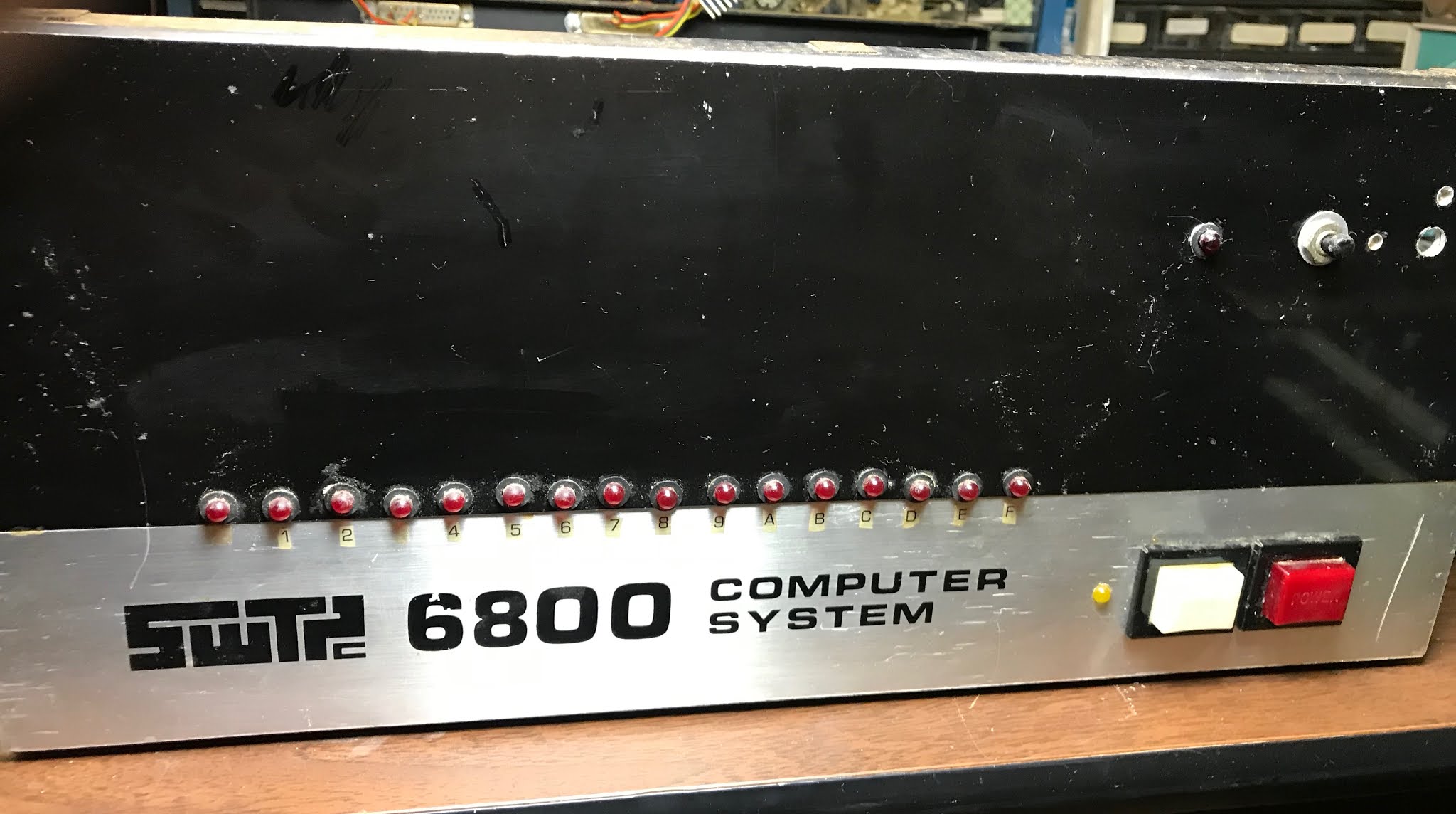 |
| Old computer veteran from November 1977, showing a few front-panel modifications. |
 |
| MP-B Motherboard |
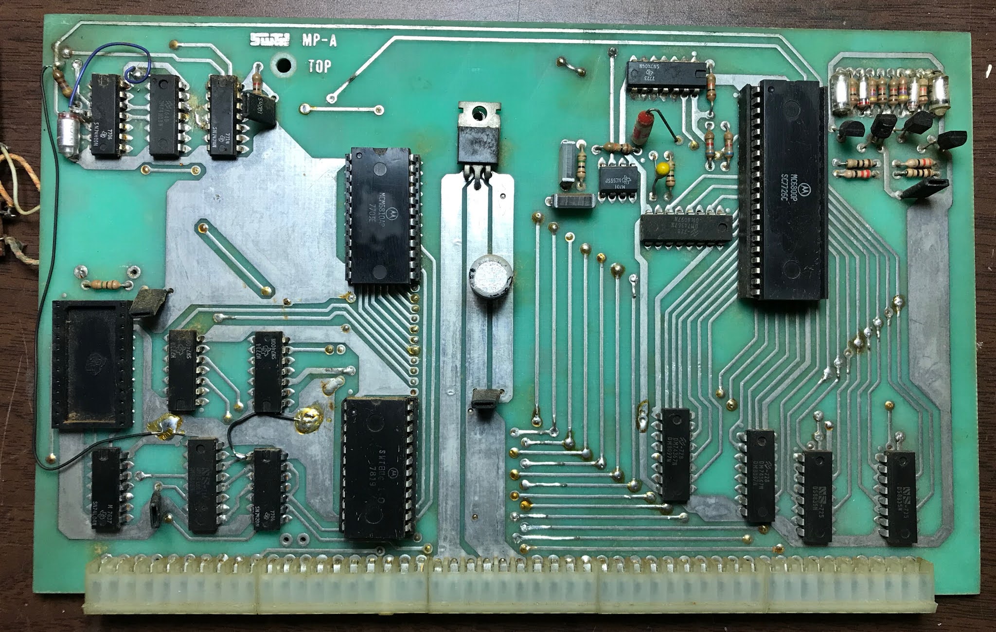 |
| MP-A CPU board |
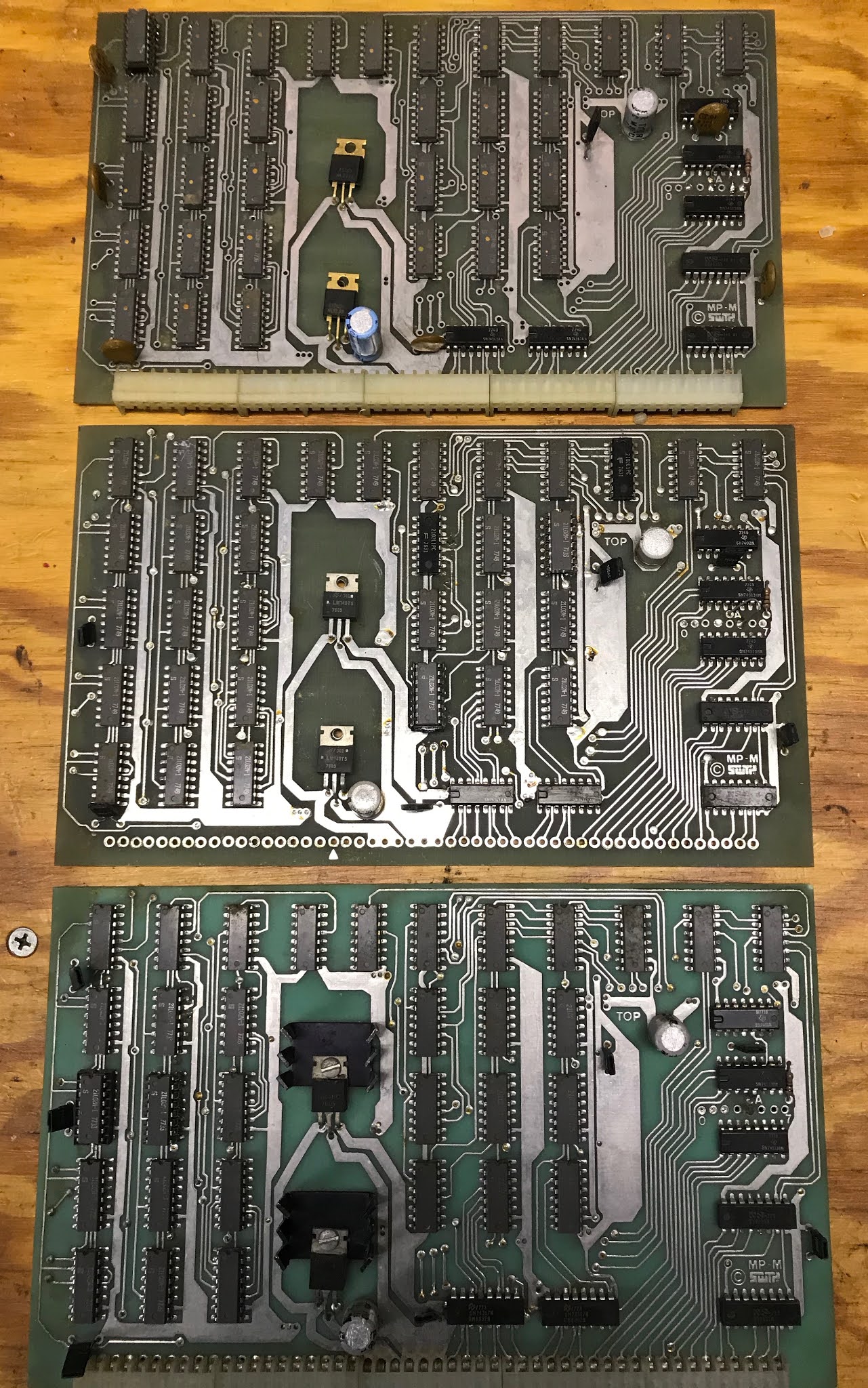 |
| MP-M 4KB memory boards |
 |
| MP-C board, modified |
![]()