I managed to get outside for just a few minutes yesterday as the moon was approaching maximum coverage of of the sun (90%) at 3:24 PM local time. I took a small shipping box and punched a hole in the side with a thumbtack. It projected a very tiny, but totally sharp image of the moon covering the sun revealing only a small crescent of sunlight. Of course, this is New Jersey after all, and clouds came in for the actual moment of maximum eclipse. But I can say I saw it. This reminded me of the eclipse of 1972, when I had my 3" refractor telescope set up in the backyard, projecting a magnified image onto a white piece of cardboard.
A co-worker managed to snap this with his iPhone.
BTW, Sean Kutzko KX9X was doing some AM Broadcast Band DXing during the eclipse. He observed that during the maximum period of darkening at his QTH, he was able to hear AM stations from over 500 miles away, that he normally can only hear at night. The D Layer was definitely affected! He recorded the AM Band during the eclipse from start to finish and will go over it in detail over the next few weeks, in order to get a better feel as to how propagation was affected.
I saw on Facebook yesterday, where Alex PY1AHD of AlexLoop fame has become a Silent Key:
It is with extreme sadness and sorrow that I share the passing of our friend and colleague Alex Grimberg (PY1AHD), AlexLoop, due to his renowned work with magnetic loop antennas. Inestimable loss for Brazilian amateur radio, an enterprising and visionary colleague - We are all saddened.
I got word from my friend that he was encouraged by your comments regarding using a local WebSDR as a receiver. He was able to hear stations on 20 Meters via the Web that he was not able to hear on his K3, due to the solar panel noise. He made three successful QSOs on 20 Meters and will most likely use WebSDR for making contacts on 14 MHz and above. Thanks for your encouragement! I'm very happy for him - he had been disappointed (that's putting it mildly) with his situation. It's good to know he can be on the air again.
My KM4CMT EFRW UNUN kit was delivered yesterday. I hope to have it built and ready to go for "Amateur Radio Day At The Library" on April 20th. If I don't have it ready, I'll probably employ the PAR ENDFEDZ or perhaps the EARCHI EFRW that I already have in the backpack. It's not that the kit is a complicated build - far from it. It's a matter of finding time. The next few weekends are really filled up now that lawn mowing season has started up again.
If you haven't heard about it, Ken WA4MNT has a great website QRPBuilder.com. He offers some neat items in kit form. One that has me especially intrigued is his QX1 antenna, which is an alternative to Elecraft's AX1 and AX2 antennas. I'm going to paste in Ken's description of the antenna:
The QX1 Antenna kit, is a small, ultra portable vertical 40m, 20-10m antenna with a male BNC connector and telescoping whip, rated at 20W. It is resonant on the whole 40m band with only a whip length adjustment. With a tuner, can be used on the 20m through 10m.
All the holes are pre-drilled and tapped. Assembly requires winding the coil, a little soldering, and some mechanical assembly. The tools required for assembly are a Phillips screwdriver, forceps or needle nosed pliers, wire cutters, soldering iron, and some rosin core solder. Depending on your experience, it can be assembled in about an hour. On a difficulty scale of 1 to 5, 5 being the most difficult, this is rated at 2.
The BNC Antenna Mount/Adapter kit is a versatile antenna mount with a nylon clamp included. This design allows small BNC terminated antennas to not mount on the output connector of the radio, but rather, with coax, to a more advantageous position. It is ideal for quick setup, field and SOTA operation. We have listed this as a separate kit because, some users already have an antenna like the Elecraft AX-1, MFJ-18xxT series, or similar homebrew antennas that are terminated with a male BNC connector. The strong clamp permits mounting to a apartment or patio railing, picnic table, or even a tree branch. There is a connection point for radials or a counterpoise with captive stainless steel hardware.
Assembly is easy and only the most common tools are needed and a 1/4″ drill. On a difficulty scale of 1 to 5, 5 being the most difficult, this is rated at 1.
I like my AX1, but I sure wish this had come out a few months ago. It's a much more affordable alternative, and with inflation the way it is nowadays, who doesn't need to stretch their $$$ as far as they can?
In addition to this nifty kit, Ken offers paddles, an audio amplifier kit and even a kit that will allow you to use normal earbuds/earphones on a crystal radio. Again, I'm not affiliated with QRP Builder in any way, shape, fashion or form; but when I see a site that offers items that I think you folks may be interested in, I'll showcase them here.
I'll see something that is "new" to me - only to see that it has been thoroughly reviewed and talked about by Tom K4SWL, Alan W2AEW and Mike K8MRD. This one has me enthused though, and you have all probably heard about it by now. But if you're like me and you've missed the bus, here's an antenna solution that has me pumped up. The KM4CFT EFHW and EFRW.
If you go on YouTube and search on KM4CFT, there are numerous videos about this antenna. Watching Mike's video shows how easy it is to build and use. I love antennas like this that are simple and are fast and easy to deploy. When you get to a park, POTA or just your local round-the block park, you want to operate and not waste precious minutes getting your aerial ready to go.
Remember the old Lays potato chips - "Betcha can't eat just one!"? Antennas are just like that - "Betcha can't have just one!" Whenever SPARC holds an on-the-air event and the subject of antennas comes up, I always hear "Don't worry! Larry and Dave (KD2FSI) have everything we'll need." I'll be ordering one of these from eBay really soon to add to my antenna arsenal.
By March 1988, the MC6809E V1 card I designed in 1983 needed updates. I built an entirely new card with new features intended to run OS-9 more effectively.
CPU
A MC6809 chip simplified things with the on-chip clock oscillator. The chip handled M.RDY without extra logic, and the rising edge of the Q clock did not need delay.
Memory
The MC6809E V1 card had no on-board RAM. There wasn't room. By 1988, a number of manufacturers had 32 KB static RAMs in 28-pin packages. 64 KB of memory is realized with a couple of chips.
For the V2 board, I allowed for eight chips, totaling 256 KB of memory. This was a good compromise between cost and the space available. The memory is logically separate from the rest of the card -- decoding from the physical address and data bus, using appropriate buffers. In this way, the memory can be accessed by a bus master other than the CPU. It responds to physical addresses C0000-FDFFF or FEFFF, jumper selectable. For years, it held two chips -- 64 KB on the board -- with only 56 KB accessible. The six remaining chips were added recently, making 248 KB or 252 KB accessible.
Buffering
20-pin bus driver chips reduced the chip count, even with two sets of bus drivers, one for the CPU, and one for the memory array.
Program ROM
The design allows for a much larger ROM. The MC6809E V1 card originally had two 2KB 2716-compatible sockets -- one for a ROM and another for ROM or RAM. To make swapping OS-9 and BBUG easier, I changed this to a single 4 KB 2732-compatible ROM socket
For the MC6809 V2 board, the ROM can be a 2764, 27128 or 27256-compatible device, holding 8 KB, 16 KB or 32 KB, respectively. The larger ROM permitted more OS-9 modules to reside there, if desired.
As built, a 2764-compatible EPROM is used, containing a BBUG image in one 4 KB half, and the OS-9 ROM image in the other 4 KB half. A jumper selects which half is active. This is much easier than swapping chips to go between BBUG and OS-9.
Accessing the correct amount of the ROM requires clever decoding.
Decoder
A hard-wired decoder would limit the flexibility of the system, and it would be complex and difficult to change. Rather than discrete logic, the decoder consists of a Cypress Semiconductor CY2C291 2Kx8 EPROM. This is a fast device with a 70ns access time. The CPU address lines A5 to A15 are connected directly to A0 to A10 on the chip. The decoder is enabled with the logical OR of E and Q, which asserts during three quarters of the memory cycle. This way, the eight data output pins can be used as decoder selects programmable on every 32-byte segment of memory.
Three select lines are used: one for bus access (including the on-board memory array), one for the program ROM, and one for the DAT. Each select line is pulled up to +5v. Placing a 0 bit in the decoder ROM data array makes the select line active for that 32-byte memory segment.
Modifying the memory map becomes a simple matter of programming the decoder ROM. I programmed the following logical memory map:
0000-EFFF - Bus
F000-F77F - Program ROM
F780-F7FF - Bus
F800-FFFF - Program ROM
FFE0-FFFF - DAT (writes only)
This configuration is compatible with the existing ROMs for BBUG and OS-9, which require I/O at E000-E07F. It has 4KB of program ROM, except for the hole at F780-F7FF. This hole deserves a bit of explanation.
I/O Port Address Migration
BBUG occupies the top 2 KB of ROM. The OS-9 ROMs take up nearly 4KB. However OS9p2 doesn't use the last 128 bytes of that space. This unused space became an alternate location for the I/O ports. If the I/O ports moved from E000-E07F to F780-F7FF, the MC6809 could use RAM in the logical E block (E000-EFFF), for a total of 60 KB of RAM, up from 56 KB.
Moving the I/O address requires motherboard decoder changes and software changes to the BBUG and OS-9 ROMs, as well as revision to Flex09 and OS-9 I/O configurations. The V2 board decoder ROM would work with the existing motherboard, or with the motherboard and ROMs altered for the new I/O addresses.
Larger ROM
Once the I/O addresses are moved, the decoder can be reprogrammed to allow for more ROM space. This opens the option of moving OS-9 modules into ROM. The decoder allows the lower limit of the ROM to be changed in 32-byte increments. This allows an OS-9 system to be entirely in ROM. OS-9 would start from the reset button without requiring a boot disk.
DAT
Back side of MC6809 V2 card.
The DAT configuration is similar to the MC6809E V1 board, with one important difference. In the SWTPc MP-09 board, as well as my V1 board, the outputs of the DAT are inverted on the lower four bits (A12-A15), but non-inverted on the higher four bits (S0-S3).
This means that values programmed into the DAT must be one's complemented on the lower four bits (A12-A15), with the higher four bits (S0-S3) not complemented.
For the V2 board, all eight bits of the DAT are inverted on the bus. Thus, the value programmed into the DAT is the one's compliment of the highest eight physical address bits (A12-A15, S0-S3).
Which makes programming correct DAT values simpler, since the entire byte is complemented.
I introduced a hardware bug in the DAT decoder. More on this later.
Building
Rather than wirewrap, I opted to try something new. A technician from work gave me a couple of 3M Scotchflex Breadboarding kits. This breadboarding system was brilliant. Chip sockets connected to IDC pins. Wiring is accomplished by forcing wire-wrap wire between the IDC pins with a special tool.
It is way easier than wire-wrap, because there's no tedious cutting, stripping, threading and winding of wire. One lays the wire down and pushes it on to the pins. Wiring several connections in succession, such as with a bus, is a breeze. The results also look great. The IDC pins are low profile, so there's less chance of shorting a connection than with wire-wrap.
It's sad 3M discontinued this product. It was great. 3M has since re-used the Scotchflex brand on three other products.
Fixing the Bug
The MC6809 V2 board worked great. There were no wiring errors. I did find a problem with the DAT.
In the default BBUG and OS-9 configuration, the DAT is written once during reset and never touched. And that seemed to work just fine.
Then I started playing with an OS-9 driver called VDisk. It created a virtual disk from selected extended memory blocks. At the time, I had 56 KB of memory from the MC6809 V2 card, plus another 60 KB from the Digital Research Computers / Tanner card. That made possible a 60 KB virtual disk.
Every time I tried to access the virtual disk, the computer would crash. This took a while to track down.
I eventually realized the new decoder did not take into account the clock cycle when accessing the DAT. Transients on the R/W* line early in the clock cycle could cause bad data to be written to the DAT. After I added the missing gate, the Disk driver worked perfectly.
Usage
Like the MC6809E V1 board, this V2 board was exactly how I wanted it. There are only two jumpers.
The jumper at the top edge of the board selects the 4KB portion of the EPROM. This makes it easy to switch between OS-9 and BBUG. No more hassle of changing out chips - just move a jumper.
The jumper in the middle of the board, just above the decoder ROM enables the FE000-FEFFF block of on-board memory. This would be installed once the motherboard I/O addresses are moved out of the E-block of memory and would allow 60 KB of RAM to be used.
Future
Moving the I/O addresses out of the E-block gains 4KB more usable memory for OS-9. Perhaps I'll try that in my retirement.
Another fun project would be to put a full OS-9 Level I system into ROM. Unfortunately, all of the essential modules take up just over 16 KB of memory, so the division doesn't fall on a natural 4 KB boundary. This might cause a conflict accessing extended memory with the DAT. I'd also have to figure out how to program the decoder ROM. There are not many EPROM programmers that can program the Cypress Semiconductor CY2C291 devices, and I no longer have access to the ones I originally used.
OS-9 Level II
This design works well for OS-9 Level I. To run OS-9 Level II, which allows each process to have a full 64 KB address space, requires more hardware. First, a second set of DAT memory chips allows the user and supervisors states to have separate memory maps. Second, a means of switching between those maps automatically -- like when servicing and returning from interrupts. Third, would require ROM to be accessible from an extended memory address, and then mapped into the supervisor space.
Those requirements go beyond the scope of this design. Perhaps there's room for a V3 board. All of this assumes access to a copy of OS-9 Level II, which may be difficult to find.
To work on OS-9, I borrowed some 5 1/4" drives, and used the SWTPc DC-2 controller. This allowed me to boot up OS-9. Single-sided, single-density, 40-track diskettes hold about 100 KB -- they were quite limited on space.
Running OS-9 on single-sided, single-density 8" disks, the situation was a little better, as each drive has about 300 KB of storage. But my two-drive system was limited. Plus, I was something of an island. None of my friends using OS-9 had 8" disks, so I couldn't exchange data with them. It was time to consider 5 1/4" drives.
5 1/4" disk drives went through considerable evolution since their 1976 introduction. The early drives were single-sided, single-density with only 35 tracks. By 1987, double-sided, double-density drives sporting 80 tracks were common. These disks could hold about 640 KB, more than twice what my single-sided, single-density 8" drives held. (And more than single-sided, double-density 8" drives could as well)
Disk Controller
In August 1987, I designed a 5 1/4" floppy disk controller. The 5 1/4" controller is very similar to the 8" design, with appropriate changes for the disk interface.
A MOTOR ON* signal is generated any time the WD2797 is accessed, with a one-shot multivibrator holding that signal for 10 seconds. Another one-shot asserts the READY signal on the WD2797 after a second of MOTOR ON*. 5 1/4" disks always have the heads loaded, so HLD is tied to HLT.
Back side of 5 1/4" controller
Double-density is jumper-selectable to either follow drive select bit 7, or the SSO output. Side selection is controlled by drive select bit 6. Write pre-compensation isn't used, as it was unnecessary for 5 1/4" disks.
I built the controller the same piece of 0.1" perfboard that originally held the FD1771 disk controller for 8" disks. The board is a little bit smaller than the WD2797 controller for 8" disks, so it appears more densely packed. Wire-wrap techniques are used for the wiring, and a handful of connectors and discrete parts are soldered.
Drives
For initial troubleshooting, I borrowed the two drives and power supply from a Sage II computer from work, which I had to return. I needed my own drives.
How many drives did I need? I decided three drives would be sufficient -- one boot disk, and two working disks. This would allow me to copy disk to disk, while still having the boot disk with commands in place. (and no crazy disk-swapping for copies like the original Macintosh that had one disk drive!)
I bought two Tandon TM100-4 drives at a local hamfest. These were common surplus from Lanier word processing units at that time. When I went to buy a third drive, I could no longer find any. I ended up with a Mitsubishi M4853 drive. The specs of the drives are virtually identical, except the Mitsubishi is a half-height drive.
Drive Cabinet
5 1/4" Drive Cabinet
Finding a cabinet to house three drives was a problem. New metal cabinets are very expensive, particularly in larger sizes, and I couldn't find anything suitable on the surplus market.
September 1987, I built a wooden cabinet to proper dimensions for three TM100-4 drives. I used 1/4" plywood, reinforced at the corners with 1x1/2 strips. The bottom, back, sides and one quarter front panel are all glued together as one unit. The top screws on to the four corner posts. The finished unit is quite sturdy.
As originally built, the cabinet was plain unfinished plywood. I recently sanded and finished it with a couple of coats of polyurethane.
Inside the box, plenty of room.
Power comes from a 12 volt, 5 amp supply. 5 volts is provided from a single LM7805 regulator mounted to that supply. In retrospect, the LM7805 might be a bit over-taxed. I suspect the drives draw less power than their maximum specifications. Heat is removed from the cabinet by a small (but noisy) muffin fan on the back panel.
A power switch and neon pilot light round out the front panel, giving a clear indication the unit is on.
The controller and drives work great, easily formatting double-side, double-density disks using 80 tracks.
Drives & Software
In April of 1989, I revised all the disk drivers to handle double-density, double-sided drives. The BBUG monitor "D" command code was updated to look for double-density sectors, and the boot loader for Flex09 updated to read double-density, double-sided disks.
For OS-9, I modified an existing driver (FD2) for the Processor Technology PT69 to work with my disk controller and created a new boot disk with several drive descriptors. The drivers and descriptors allowed for 40-track disks (which required double-stepping of tracks, and adjusting the track register), and SWTPc format, where track 0 is formatted single-density -- as well as the standard, double-density, double-sided, 80-track format.
I updated the Boot module to handle double-density, double-sided disks and burned a new OS-9 ROM.
The result is a smart, efficient unit roughly the same size as the SWTPc 6800 Computer System cabinet. The fan is a little noisy, but was typical for the day.
Future
The Tandon and Mitsubishi drives only require 250 ms to get up to speed after MOTOR ON*. I can shorten the timing on the one-shot driving the READY signal.
If I can manage to find a second Mitsubishi M4853 drive, four drives would fit into the cabinet. I'd need to add a second LM7805 regulator for the 5-volt supply, and split the 5-volt output across two drives for each.
One limitation of the WD2797 is the track to track and head settling time. These drives can move track to track in 3 ms and need 15 ms for the head to settle. The WD2797, using a 1 MHz clock for 5 1/4" drives, can only do 6 ms and 30 ms, respectively.
Western Digital did manufacture another device, the WD1772-00. This was a 28-pin floppy disk controller for 5 1/4" drives that is software compatible with the WD179x and WD279x devices. The WD1772-00 allows faster track to track and head settling times -- up to 2 ms and 15 ms.
The biggest problem is finding one, as the WD1772-00 wasn't used in a lot of designs, and Western Digital stopped manufacturing them over a decade ago. Might be interesting for a V3 floppy disk controller card.
One of the first ham radio specific kits that I built was a dummy load from QRP Guys. I keep it on my desk. It’s two PCBs with a shedload of resistors sandwiched between. It is simple. It is brutally effective. And the other day, it was invisible. I have no idea how it wound up in the drawer that it did, but I was absolutely unable to locate it for about two weeks. This is more than just a case of “It’s behind the milk”. This was almost nefarious.
My original dummy load from a QRP Guys kit wrapped in red electrical tape to make it easier to see. Hmm.
Yeah. I was trying to organize my office and hid it from myself.
The quick lesson was that I use my dummy load a lot more than I realized. I keep it on the desk so I can slap onto a rig if I want to apply power and play with settings or do much of anything that might inadvertently trigger a TX.
With my trusty dummy load missing, I did the only thing that made sense: I ordered another. But this time, I went with the Digital Power/SWR Meter with Dummy Load Kit from QRP Guys. It was a great experience with the first one, why not go back for more?
The kit arrived and I put it on my bench to assemble in the coming week. I then went into my office, opened a drawer to grab some electrical tape and there was my original dummy load.
Nice.
Well, with the kit in hand, there was work to be done. Given that the weather in NE Ohio can be pretty awful this time of year (I find that radio gear is more amenable to snow than misty, cold, intermittent rain) I decided to go to the bench and get it together. The process was swift. As with all of the kits of their’s which I have assembled, this one was well documented and easy to assemble. It did involve winding a transformer (not my favorite passtime given I have rather large hands) but it was painless.
The assembled PCB with all parts in place.
The kit even powered up the first time!
This was my first kit project where I got to use my 3d printer to make an enclosure. There is a link to the various design files on their site and the model is perfect. My Anycubic Vyper took about 10 hours or so to print the top and bottom in one go. I chose a rather strange lemon yellow color for the case so that it will be easy to locate. Nothing else I own is that weird color. With sliders and a button printed, the case went together pretty smoothly.
3d Printed case next to the assembled PCB.
And now I have a second dummy load that can also do double duty as a Power/SWR meter in the field (or on the bench).
The fully assembled kit inside of its enclosure complete with sliders and button.
It’s a great kit and I’m glad I got it. I’ve already used the dummy load feature a number of times and the Power/SWR meter works well. Look, it’s not an oscilloscope, but it is a Good Enough meter from a kit and does the job at QRP levels. I recommend it.
I was QRV in Gordon county briefly - only a couple of weeks. I managed to erect the 80/40/20m dipole I had up in Warren county, which previously flew over Fulton county. It was a cobbled-together mess, made from wire left over from the original 80/40m dipole, newer traps, and old insulators and rope.
Using the Mark III Antenna Launcher, I did a good job casting over a tree in the front yard. Weight sailed up over the tree and came right down beside the trunk. The 1/16" guide line went back out to the antenna launcher, and then the 1/4" nylon halyard came back over. Perfect.
At the far end, I had more trouble. Not wanting to crawl over a fence, I cast sideways to branches overhanging the edge of the yard. The first toss wasn't great, so I pulled it down. Second toss got stuck in the tree, and I lost the weight. I was down to my last antenna weight. I confidently tied it on, pulled back, let it fly, only to watch it sail off the end of the fishing line and into oblivion. Nuts.
With no weights handy, I couldn't use the antenna launcher. I opted to use a small hammer and toss the halyard over a branch about 20 feet up in the tree. At least I didn't lose the hammer.
The resulting installation sloped the dipole from about 25 feet on the south end, to about 60 feet on the north end. No matter - it would work. At least, until I could make more weights and get it higher in the air.
I used it to make about 100 contacts for the NAQP Phone in August, plus a little casual operating. Then I found most of it lying on the ground after a few windy days. Inspecting the remains showed that the wire between the 20 and 40 meter traps had broken. That particular segment was pretty old, being part of the original 80/40m dipole, and might have used wire from the ancient untuned doublet before it.
This meant that one of the 40m traps was still up in the tree. Looking carefully, I could see it about 50 feet up. Untying the rope, I could not get it to drop, and instead pulled the halyard to recover the rope. The wire ended up coming off the insulator, leaving wire and one trap stuck in the tree. Drat.
The rest of the antenna lay across the yard and lower driveway. I don't use that driveway, so I didn't think about it. However, some folks came to visit the parsonage and apparently didn't see the traps laying there. Two of the trap forms got crushed in the process. Doggone it.
I guess I have to rebuild this antenna from scratch, using new wire and traps. That will take some doing, as most of the parts are back in Gwinnett county. Plus, I have to make more antenna weights to put it back up.
In the meantime, I'm off the air in Gordon county.
WD2797 controller card for 8" Pertec drives in the Icom Peripherals FD360
The FD1771 disk controller works well with the Pertec 8" drives. The single-density drives each hold around 300 KB of data.
Single-density encoding is FM, which has regular clock pulses, with a data pulse placed between. A data pulse indicates a "1", a missing pulse is a "0".
Double-density uses Modified FM (MFM) encoding. It eliminates the clock pulses entirely, leaving only the data pulses. To keep synchronization during runs of zeros, extra pulses are inserted between each pair of zeros. Encoded in this way, the clock can be recovered from the data pulses alone.
Western Digital followed the FD1771 with the WD179x chips, which support double-density with a two device solution. The later WD279x chips offer the same features on a single device. Double-density allows 500 KB on the same disks, with the data transfer rate also doubled.
WD2797 8" Controller
Back side of the 8" controller
September 1986, I built a new controller using the WD2797 to support the Pertec FD400 drives. While the drives were designed for single-density, I hoped they would work using double-density.
In keeping with my other home brew cards, it's built on a piece of 0.1" perfboard with the Molex connectors epoxied to the bottom edge. Wire wrap sockets are used.
Naturally, I broke out the WWARP program I used years before to build the MC6809E V1 card.
The WD2797 design borrows from the FD1771 design. I kept the latching data bus buffer, but eliminated the redundant data bus buffers in front of them. The WD2797 performs the clock/data separation, which eliminates several gates. Fourteen total chips on this board, whereas the FD1771 board used more like eighteen.
Double-density is enabled through an option jumper. The SWTPc DC-4 controller used the SSO output to drive the DDEN* pin through an inverter. (SWTPc offered double-density before double-sided disks) One side effect of using SSO is the sector address markers will have side 0 for single-density sectors and side 1 for double density sectors.
Other designs used bit 7 of the drive select latch, controlled through software. SSO isn't connected to anything, as the Pertec drives only have one side.
A jumper at the top of the card chooses the DDEN* signal source: the SSO pin, or bit 7 of the drive select latch. Both paths go through an inverter, so double-density is selected with a 1 on either the SSO pin or bit 7.
Bit 3 of the drive select latch controls ENP - the pin for write pre-compensation. Generally, ENP would connect to the TG43 output of the floppy drive interface. Using a separate bit allows write pre-compensation to be enabled or disabled at any time, through software. I didn't know if write pre-compensation would be required or desired. It seemed like a good plan to allow write pre-compensation on any track, since the Pertec drives weren't designed for double-density.
Reading the drive select latch address returns the state of the INTRQ* and DRQ* pins, on bits 7 and 6, respectively. Using these separate bits allows more efficient loops than reading and interpreting the status bits of the WD2797. The SWTPc DC-4 introduced this feature, and is common to controllers of that era.
The WD2797 calibration starts by grounding the TEST* pin and checking three signals with a scope. A set of four pins at the base of the WD2797 chip bring these signals out making calibration easier.
To support the new controller, I re-wrote the Flex09 disk drivers to allow double-density operation.
Do the Pertec drives work at double-density? I don't know. Supporting double-density meant re-writing NEWDISK to initialize in double-density format. Before I figured that out, my interest shifted from Flex09 to OS-9, and I did not complete that project. But the card works great with single-density.
September 1985, I purchased a Kenwood TS-430S and became more active in amateur radio. In the apartment where I was living, I snuck wires out of a second floor window and began to make contacts.
In October, I got the notion to try some Radio Teletype (RTTY). I built a demodulator using a circuit I've forgotten. Perhaps it used a couple of NE567 chips. Having a demodulator, I needed to translate the five-level Baudot characters into ASCII that I could display on the terminal.
(I purchased a Wyse 85 VT-220 emulator terminal in August of 1985, so I was no longer constrained by the 64x16 screen and 1200 bps limitations of the CT-64)
RTTY Decoder
I wrote a program for Flex09 to decode 45 Baud RTTY by bit-banging a PIA pin. I couldn't use the MC6850 ACIA, because it does not support 5 bit characters.
A delay loop established character timing:
LOOP LEAX -1,X BNE LOOP
Each pass through the loop consumes 8 clock cycles. With the right value loaded in X, fairly precise timings could be accomplished. A value close to 250 would be 1 ms on a 2 MHz machine. By calling this loop repeatedly, timings of 11 and 22 ms are measured.
I connected the demodulator output to PIA Port B, pin 0. The program looks at this pin, waiting for a zero. Finding one, it calls the delay loop for 1 ms and checks again. If the pin is still zero, it waits 10 ms and checks Port B pin 0. A continued zero at this point indicates a start bit. The 11 ms total delay places us right in the middle of the start bit.
The next sequence waits 22 ms and then samples of value of Port B, pin 0. It does this five times. These samples are shifted into a byte value, which used to look up an ASCII character in one of two tables -- one for letters, and one for figures -- according to the shift mode. This character is then sent to the terminal, and we go back to waiting for a start bit.
The resulting program is about 300 bytes long. Despite the simplicity, I had little success decoding RTTY signals.
In hindsight, there are several reasons for this.
Decoding signals off the air that might have been noisy.
Demodulator circuit was completely untested and might not have worked.
No experience with RTTY, so signals might not have been properly tuned.
Precise value of the 1 ms time delay not known. I used values of 230 and 240, allowing cycles for other program logic.
At some point, I distinctly copied "RY RY RY RY RY RY RY" from someone, but not much else. Later, I figured out this meant my program, at least, was working.
Hardware Solution
In November 1986, I decided to use serial chip that could do five-level Baudot. The MC6850 only allows 7 and 8 bit characters, so I needed a different chip. The NS8250 could do 5, 6, 7 and 8 bit characters, and sports a programmable bit rate generator for all the common RTTY rates. Hence, I added an NS8250 UART to the baud-rate generator board.
Funny, though -- I never wrote software to use the NS8250. In February 1989, I removed the NS8250 and its associated circuitry.
I didn't become active in RTTY on the air until 2005, using Cocoamodem.
Some time in 1985, I had one of those moments I regretted.
I'd gotten my MC6809 system running in late 1983, running the Flex09 operating system on 8" floppy disks. I had a full set of documentation for several pieces of hardware and software. My new job kept me busy, so I didn't have much time to work with my system at home.
August of 1984, I began programming the Macintosh at work. We published our first product in March of 1985. The Macintosh was a revelation -- it completely changed the metaphor for computing. I saw early on that it was the future. But, I couldn't afford one right away. I wouldn't buy my first Mac until the summer of 1987 -- a Macintosh SE. I've only purchased Macintosh computers since that time.
In the late spring of 1985, I prepared to move to a new apartment. I had bulky boxes of documentation in my closet. I figured that I'd never do anything more with that MC6809 system -- the Macintosh was the future.
I threw nearly all of the documentation away.
Two months later, in the new apartment, I regretted my decision. There were things I could do with my MC6809 computer. I had to replace the missing documentation.
To this day, I'm not sure I found replacements for everything I had.
I graduated from Georgia Tech in the fall of 1983 and got a full-time job. By 1984, 20 KB of memory didn't seem like enough for the MC6809E V1 board. My attempt to expand the 8 KB MP-8M to 16 KB didn't work. And I never built the dynamic RAM circuits I designed. I wanted more memory.
Digital Research Computers marketed an SS-50 card designed by Tanner Computers in the early 80s. It sported thirty-two sockets for 2 KB RAM or ROM chips. These 2716-compatible chips were quite popular at the time.
I bought a kit for about $225 with a full 64 KB of RAM in June 1984.
Assembling the kit was straightforward, along the lines of the SWTPc kits. The board worked right away, with no soldering issues -- largely due to the excellent solder mask on the board.
For SS-50 systems, this board has several flexible options. The first 48 KB presents as three 16 KB banks that are enabled individually. Each 2 KB segment in the top 16 KB is enabled individually, allowing one to navigate conflicts in the C, D, E and F blocks of memory. This allowed for I/O on the motherboard, or perhaps RAM or ROM on the CPU board.
The board supports extended addressing on the S0-S3 pins. When enabled, the entire board responds as one 64 KB block. Each socket can contain either RAM or ROM chips, selectable by the jumper next to each chip.
Initially, I used this board without extended addressing as a 56 KB board. I later enabled extended addressing to access the full 64 KB, after modifying the MP-B motherboard to decode the 20-bit address for the I/O slots. This allowed me to use that 8 KB of RAM for a virtual disk drive, briefly.
I discovered some extended memory issues between BBUG/Flex09 and OS-9, so I disabled the MP-B decoding.
As pictured, the board has the E000 and E800 blocks disabled, with F000 enabled, and F800 disabled. This configuration was appropriate for the MC6809E V1 CPU board and MP-B motherboard without the 20-bit address decoding, although, technically, the E800 block could be enabled, and the F000 block would not be accessible after I modified the MC6809E V1 CPU board for a 4K ROM.
SWTPc 6800 front panel, sporting sixteen LEDs. Each LED indicates a 4 KB address block access. You can also see a yellow power LED was added.
The SWTPc 6800 Computer System sports a rather spartan black and silver front panel. Unlike contemporaries of its day, there were no lights.
I'd already modified the front panel of my computer. I mounted the CIS-30+ cassette interface inside the case, which accounts for the assortment of holes in the upper right. There's a yellow power LED next to the reset button. Before I went to the ISEF 1979, I replaced the power switch with a key switch. I added the yellow LED so I could tell when the machine was on.
While building the MC6809E V1 board, I decided to add some lights. Hooking up LEDs to the address bus didn't seem useful, since addresses change quickly. Plus, the DAT complicated the issue -- do you show logical or physical addresses?
I ended up with a simple solution. Running the top four CPU address lines into a 4:16 decoder, each LED indicator represents a logical 4 KB address block. This connects to the CPU board directly, before the address signals enter the DAT.
Board holding 74LS154 and LEDs.
I drilled the front panel for sixteen LEDs. On the backside of the front panel, I mounted a 74LS154 4:16 decoder and wired up the LED cathodes. The board is held in place by the LED wires. A 16-pin ribbon cable goes back to the CPU board and attaches to a socket.
This socket has address pins A12-A15 from the CPU, the VMA* signal, the DAT write decoder signal, +5 volts, and ground. The VMA* and DAT write signals go to the two Enable* pins on the 'LS154. This means the address must be valid, and not writing to the DAT to enable.
The LEDs anodes are connected together to a resistor to +5 volts. Originally, this was a 470 ohm resistor. I found that the LEDs lit very dimly. Each LED is not asserted all the time. VMA* is not asserted at all times, and pulses every clock cycle, which limits how bright the LED can illuminate. I decreased the resistor value and experimentally arrived at a value of 22 ohms.
The resulting front panel is informative. I can see when the CPU is busy-waiting on I/O ports, if it is crunching away at some calculation, or if it has crashed entirely. And if the CPU executes a CWAI instruction to wait for interrupts, all the LEDs go dark.
The bare board that held the HB 6809 V1 circuitry. Waiting for the next SS-50 project.
In computings early days, advancements happened quickly. Which mean purchases went out of date quickly. I built my SWTPc 6800 Computer System in November of 1977. In 1978, Motorola introduced the MC6809 processor, and by March 1979, SWTPc had the MP-09 CPU board available.
MC6809
For those who programmed the MC6800, the MC6809 fixed many problems. It sports 16-bit arithmetic operations, more index registers, many additional addressing modes and a very orthogonal instruction set. It was a powerhouse of an 8-bit processor. Early chips were costly, and the marketplace moved quickly beyond 8-bit chips to 16-bit ones. The MC6809 never became popular enough to dominate the market. For that brief time in the late 70s, it was the most powerful 8-bit processor. I wanted one.
Georgia Tech Symposium
In early 1983, Georgia Tech hosted a symposium where Terry Ritter, one of the designers of the MC6809 spoke. I attended, and the room was packed. Ritter talked about the design decisions that went into the architecture of the MC6809, about the importance of reusable software and position-independent code. Their design lead to the creation of BASIC09 and OS-9.
At the time, I wasn't much interested in any variety of BASIC, so I didn't pay much attention to OS-9. I should have.
The last of Ritter's talk was about an unannounced product, termed the General Motors Custom Microprocessor (GMCM). It built on the foundations of the MC6800. At that time, GM was using the MC6802 in their vehicles. The GMCM added some features to the MC6800, such as 16-bit arithmetic, an extra index register and both multiply and divide instructions. (Divide was something that the MC6809 did not have) But the GMCM lacked all the complex, orthogonal addressing modes of the MC6809. The next year, Motorola introduced the MC68HC11.
MP-09
SWTPc offered the MC6809 with the MP-09 board. The MP-09 draws from the design of the MC6800-based MP-A2 board. Both have four 2716-compatable sockets that can hold 2 KB ROM, PROM or EPROMs. While the primary difference is the CPU, there are other differences:
SS-50 bus changes for the 6809 processor
NMI and RESET switch connections relocated to a CPU board connector, which frees up two bus lines for BUSY and M.RDY, respectively
ROM socket at address F800
ROM/RAM sockets at address E000, E800, and F000
No on-board RAM. (the MP-A and MP-A2 had 128 bytes of RAM)
16 bytes of writable memory at address FFFx that translate the top 4 bits of address
This last feature is known as the Dynamic Address Translator or DAT. The DAT uses a fast 16x4 bit RAM - the 74LS189 chip. It sits between the top 4 address lines A12-A15 of the CPU and the physical bus. Thus it translates address values in 4KB blocks. It is the reason the MP-09 has no on-board RAM. The ROM monitor SBUG-E, on reset, scans addresses to determine which 4 KB blocks have RAM. It then writes the DAT to position those 4 KB blocks as desired. The first block is relocated at D000-DFFF, and the second block at C000-CFFF. These two blocks are used for the stack, and any operating system such as Flex09. The rest of the memory blocks are arranged from address 0000 upward.
The board has a socket for an additional 74LS189 chip for the DAT, which adds the four higher-order bits to the DAT RAM. This extends the address bus with four more lines (S0-S3) allowing the MC6809 to address 1 MB of memory. The S0-S3 lines take the place of the bit rate signals on the SS-50 bus, so these signals have to be supplied elsewhere for the SS-30 bus. SWTPc did this with their MP-MB motherboards, a component of the SWTPc S/09 systems.
The MP-09 board runs on the original MP-B/B2 motherboards with modifications. More on these later.
During my years in college, I eagerly wanted to upgrade my computer to the MC6809. I obtained a copy of the SBUG-E source code and studied it. By April of 1981, I modified SBUG-E, removing code for features I didn't need and adding some features of my own. I called my monitor BBUG. I used a cross-assembler on the Pr1me minicomputers to build my code. But I could not run BBUG without hardware.
MC6809E V1
My last months at Georgia Tech, I took a required course that involved building a working microprocessor system. It had to have ROM, RAM and I/O. Many of my colleagues used the computing laboratory that provided prototyping plugboards and components for their circuits.
This was a challenging course for many computer science majors. It was their first experience with digital logic. And the prototyping plugboards had been used and re-used so many times that their connections were not always reliable. This made it difficult to determine if problems were programming bugs, wiring errors, or just flakiness in the hardware.
I didn't relish dealing with flaky prototyping boards. I had fulfilled many of the requirements of this class when I built the SWTPc 6800 system in 1977! This seemed an opportunity to create my own MC6809 processor board.
I had read articles about the MP-09, and had copies of the schematics, which I studied in-depth. There were electronic parts stores and friends around Atlanta where I could obtain components. It seemed right.
MC6809 V1 Design
April 1983, I drew up schematics. My design borrowed from the MP-09, and included the DAT, but there were several differences.
I did not include an MC14411 bit rate generator or crystal. I intend to use extended physical memory right away. I moved the bit rate generator and crystal to a card plugged into the SS-30 bus. There were no bit rates on my SS-50 bus, only S0-S3 address lines.
Instead of the MC6809 chip, I opted to use the MC6809E. The MC6809 has a built-in clock oscillator and bus control logic. The MC6809E requires an external oscillator as well as a few chips to handle bus control for things like DMA. In trade, it has an LIC (Last Instruction Cycle) and AVMA (Advance VMA) pins. I made use of AVMA in my design.
Instead of four 2716-compatible 2KB sockets, I only had two. A ROM at Address F800, and ROM or RAM at address F000. Having ROM or RAM at E800 or E800 didn't make sense to me, since those addresses conflicted with the I/O ports used by SBUG-E. (In October 1986, I would revise this board to use a single 2732-compatible 4KB chip, covering F000-FFFF)
The memory map for this design was pretty straightforward:
0000-EFFF - accessing off the CPU board to the SS-50 bus
F000-F7FF - ROM/RAM socket #1
F800-FFFF reads - ROM socket #2
FFF0-FFFF writes - DAT RAM
I had no option switches or jumpers in this design. It was exactly how I wanted.
Dynamic RAM Design
The same month, I drew diagrams for dynamic RAM boards. One was a 64 KB board using 4116 chips. Another design provided 256 KB memory using 4164 chips. I intended to add one of these boards to my project. The 4116 design was complicated, with multiple voltages involved. The 4164 design was simpler, but the chips were more expensive. I never build either design.
MC6809E V1 Building
Although I had made some simple PC boards, creating one for the MC6809 design was outside my skill set. Plus, it would have been expensive for my student budget. I had constructed a seven-chip CMOS keyer in 1979 using point-to-point wiring. That was difficult. I built a duplicate keyer for my brother in 1980 using wire-wrap construction. Wire-wrap was a heck of a lot easier. Plus, I already had the tools. A friend supplied wire-wrap wire and sockets and I was in business.
Wiring a design this complex directly from the schematic worried me. Wiring mistakes were easy to make, and hard to track down. Then a classmate asked to join my project. Denise Messerschmidt worked with me in the Users Assistance office at the Computer Center, and she didn't want to have to fuss with the flaky prototype boards either. She asked if she could help, and I figured should could do the wiring of the hardware. This required good instructions.
I solved that problem with a bit of software. I used the LL(1) parser generator written by fellow student Roy Mongiovi and defined a 28 production computer "language" that described the chips and devices and the wiring between them. Given a well-described design, my program produced three lists as output.
The device list showed each device and all of the signals connected to each pin. A device was either a chip or a plug. Chips listed two pins to a line, just as it would appear on a DIP device. Plugs listed one pin to a line. The device list made it easy to verify the design was correctly programmed in the language.
A cross-reference list related the signals connected to each device. Another cross-reference list showed the signals by each device and pin. One would follow this final list to do the wiring. The Wire Wrap parser was about 2500 lines of Pascal code, and it worked beautifully.
The board used 0.1" perf-board, cut to 8 1/2" by 5" -- a little smaller than standard SWTPc boards. Molex connectors epoxied on the edge connected to the SS-50 bus. I installed the wire wrap sockets, and wired up the voltage regulator and the SS-50 pins, plus a handful of discrete components. That took care of everything that required soldering. After training Denise in wire-wrap technique, I gave her the board, wire, tools and the wiring list.
About two weeks later, she came back with the finished product. Every wire had to be manually stripped and wrapped. Denise had done an excellent job - better than I would have.
MP-B Modifications
The MP-B motherboard required modification to work with my 6809 CPU board. The I/O ports on the MP-B decode as eight, four byte ports starting at address 8000. The SBUG-E (and hence BBUG) monitor expects eight, sixteen byte ports starting at address E000.
The modifications aren't difficult:
Connect SS-50 A2 and A3 to SS-30 UD3 and UD4, respectively
Move the ABC inputs in U3 from SS-50 A2, A3 and A4 to A4, A5 and A6, respectively
Cut the trace on U3 pin 5 (Enable*) and connect to SS-50 A9
U5 has an unused NOR gate, connect the inputs to SS-50 A10 and A11, and the output to U3 pin 6 (Enable)
Move the U6 pin 4 (Enable*) from SS-50 bus A6 to A12
Move the U6 decode output on pin 4 (4*) to pin 7 (7*) this signal goes to U3 pin 3 (Enable*) and U5 pin 13 (Enable* for data bus drivers)
Modifications on underside of MP-B. The brown wires on the right go to the 74LS21.
To support extended addressing using S0-S3, the traces between the SS-50 bus to the SS30 bus for the bit rate lines 110, 150, 300, 600 and 1200 must be cut.
I added extended address decoding for the I/O ports. I mounted a 74LS21 4-input AND gate on a daughter board, and connected the inputs to S0-S3, the output goes to U6 pin 6 (Enable).
With these modifications in place, the I/O ports show up in memory as eight, sixteen byte ports, from physical address FE000 to FE1FF. The ports show up in memory four times in sequence, because address lines A7 and A8 are not decoded.
Bit Rate Generator
Bit Rate Generator Board
Since I used the extended addressing lines S0-S3 on the SS-50 bus, the bit rate signals must be provided on the SS-30 bus.
For this, I built a simple card that had just four components: MC14411, LM341-5 regulator, 1.8432 MHz crystal and a capacitor. You can see them lined up on the left side of the board. The MC14411 is the original device from the MP-A CPU board with a date code of 7718 - the 18th week of 1977.
Later, I added the MC6840 timer chip and the SN74LS04. At some point, this board also held an Intel 8250 UART, which is the reason for the molex connector in the upper right. But those parts have been removed. There's certainly room for an MC6850 ACIA or other I/O device on this board.
Bit rates are configured as follows:
110 = 38400 baud
150 = 2400 baud
300 = 300 baud
600 = 9600 baud
1200 = 1200 baud
This represents a good collection of rates across a wide range. As configured other rates are available on the MC14411 from 300 to 115200 baud.
MC6809E V1 Debugging
The beautifully wrapped board Denise wired didn't work.
When I built the SWTPc 6800 Computer System, it didn't work the first time, either. I borrowed an oscilloscope and figured out the issues. For the SWTPc 6800 boards, the problem was nearly all solder bridges. But those boards started with a working design. Mine was untested.
I had access to test equipment on campus, but I couldn't take any of it with me. I had to bring the whole computer and terminal into one of the computer center labs in the evenings, when the labs weren't in use. An oscilloscope wasn't enough. I was introduced to a new device, an HP logic analyzer -- although it took me a while to figure it out. Those evening sessions in the lab were very productive.
Dragging my computer and terminal in and out of he lab each day, I isolated six different wiring errors on the board. Had Denise let me down? No, the wiring errors were all in the original wiring listing! Denise had done her job to perfection -- she wired it exactly as specified.
Once the wiring errors were fixed, the debugging process went smoother. I also had to correct some defects in BBUG. At one point, I had all 24 channels of the HP logic analyzer engaged. 16 pins went to the address bus, and the other 8 to the data bus. This way, I could watch each memory cycle of the MC6809 and determine what was happening.
Eventually, I fixed the issues and had the system running. I received an "A" for the course. Denise, because of her limited involvement, received a "B", but we were both happy.
End of an Era
In 1988, I built another MC6809 CPU board. It replaced the V1 board, and once working, I stripped the V1 board down for parts. All that is left is a board with edge connectors and a voltage regulator, which you see at the beginning of the article.
Nearly five years ago, I mounted a Cushcraft A50-3S out in the yard. I figured this would work for a few months until I found a more permanent solution. This lasted way longer than I expected.
It was a good move. I worked 48 states, plus 39 countries using that antenna, despite feeding it with 120 feet of RG-8X which likely adds 3 dB loss.
In July 2021, I asked the SEDXC email reflector for advice on how to work Europeans on 6m. I heard others working them, and even heard a few myself. For the most part, however, I could not hear them, or I couldn't get them to hear me.
The first piece of advice was to get a better feed line. RG-8X is not a good choice for VHF, especially with over 100 feet. The second bit was to mount the A50-3S a little higher. It's taken me a year and a half to get there. I've finally taken the first step.
The first question: where to put the antenna? The mount in the yard used a mast concreted into the ground that originally supported a Cushcraft R7000. I considered moving it to my 50 foot tower below the Cushcraft A3S/A743. The option allowed for easy rotation, and would have been convenient. However, with antennas in close proximity at five feet away, I believed there would be too much destructive interaction. I needed a mount point further away.
View of installation.
Without room for additional towers, I opted to mount a mast against the house, about 30 feet away from the tower. This location is close to where coaxial cables exit the house, which meant a shorter feed line. An older but serviceable piece of 9913 had sufficient length, so the feed line problem was solved.
How to mount a mast to the house took a bit of figuring. I used a small 6" wall mount on the eave of the house, just below the gutter. This gives the mast enough distance to clear the gutter. The bottom of the mast sits in a pole mount on the railing of the deck blow. The mast is the same 19 feet using two 10 foot pieces of rigid EMT I used to mount the antenna in the yard.
Erecting the antenna was a little bit of a challenge. I used a rope and pulley hooked on the wall mount to raise the mast into position, then lifted the mast up on the railing. The weight of the rigid EMT made this harder.
Reflector askew
In the process, the reflector of the antenna brushed up against the roof, which knocked it out of alignment. It doesn't affect the operation of the antenna terribly much, but I will fix it eventually.
The mast bracket is not cinched on the mast, to allow for rotation. Jam nuts are used to keep the bracket U-bolt from loosening.
The result has the antenna around 27 feet (8m) high, next to the house, fed with about 50 feet of 9913. This should be a substantially better than out in the yard.
I plan to replace the mast with some aluminum tubing, as well as adding a rotator, which should put the antenna a couple of feet higher. That will also give me an opportunity to straighten out the reflector alignment.
In the meantime, I'm ready for this year's Es season in plenty of time.
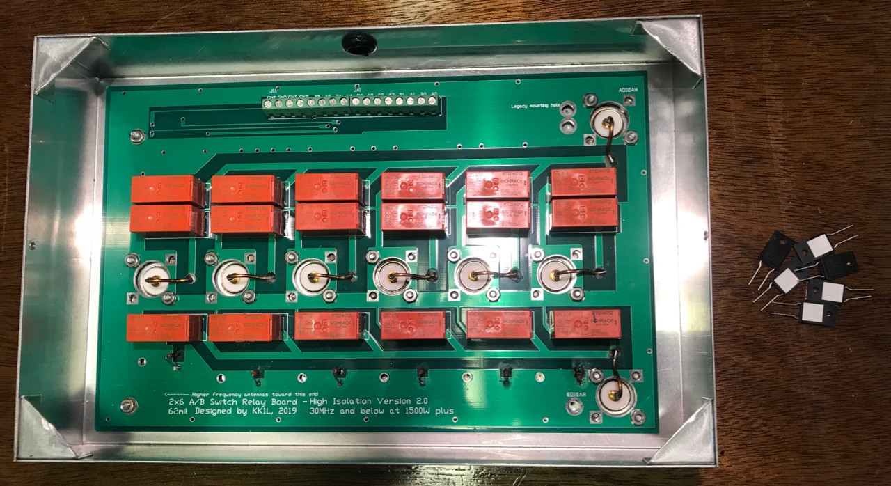
My KK1L board, showing the old resistors on the board, and the new ones on the desk.
While testing the KK1L Antenna Switch after mounting to the Single Point Ground (SPG), I noticed that some of the load resistors were no longer 50 ohms.
These resistors provide a load impedance whenever a antenna jack is not selected by either port A or Port B. This protects the antenna from static build-up as well as dissipating any coupled RF energy.
I originally used 50 ohm, 1/2 watt resistors I had on hand. Clearly they were not up to the task. On the ports for the shunt-fed tower, and the 80/40/20m trap dipole, these resistors were completely open. Both showed signs of overheating.
Most likely, these resistors succumbed to dissipating too much couple RF energy. I needed bigger ones. KK1L had 50 ohm, 50 watt resistors in his Mouser parts list, so that's what I ordered. These sorts of things come in handy, so I bought ten. Due to supply chain issues, they were back-ordered for months. But they finally arrived.
Replacing these parts is a pain. First, I had to remove the KK1L box from the SPG panel. Next, I had to remove the board from the aluminum box. Before I did that, I made sure to mark the locations the mounting screws for each resistor. To remove the board, I had to unsolder the eight connections to the SO-239 center conductors and bend them out of the way. Then came twenty-some nuts holding the board in place.
With the board separated from the box, I drilled the holes for the resistor mounting screws. I used a numbered drill bit the same size as the hole in the board to give me the largest tolerance. With the holes drilled and de-burred, my attention turned to the board.
Board with new resistors
Next step was to remove the existing resistors. Where they connect to the relays was easy, but the connections to the ground plane were harder. The ground plane tended to carry the heat away, making it hard to melt the solder without damaging the board. Getting these holes cleared of solder took a lot of effort.
Once done, the new resistors mount cleanly on the underside of the board. I oriented the resistors so the ceramic patch was toward the aluminum box. This patch does not appear electrically conductive.
After the resistors are soldered, the process is reversed to re-install the board in the aluminum box. In addition to the existing twenty-some nuts, there are also six new #4 screws and nuts to mount the resistors securely. With that in place, re-soldering the eight connections to the SO-239 center conductors completes the job.
I mounted the KK1L box to the SPG, and then re-tested all the switching combinations. This was to ensure I had connected the switching lines correctly.
I hope the new resistors are up to the job. I'll have to check on them in a few months to make sure.
The GE TDM-114 Data Set. The big toggle switch is my modification so I could turn it off.
GE TDM-114 Data Set
In the fall of 1979, I headed off to Georgia Tech and brought my computer with me to the dorms. My roommate that first quarter wasn't impressed. Nevertheless, I continued to work with the computer and learn new things.
In those days, Georgia Tech used a CDC Cyber 74 system for instruction, and one could dial into the system with a modem. I managed to locate a GE surplus modem for about $40. It was an acoustic coupler modem -- you would dial the phone manually, then jam the handset into the unit. Speakers and microphones would pick up the sounds from the phone line through the handset.
Rear View of TDM-114.
In my second quarter, I ordered a unit. When I got it, it did not work. Fortunately, it came with a manual with a schematic and troubleshooting and adjustment guide. I didn't have any test equipment other than a Volt-Ohm Meter (VOM). I don't remember how I fixed it. With youthful curiosity and dogged persistence, I managed to find a diode that didn't appear to be working, replaced it, et voila! It worked.
Manual with unit.
This was a BELL 103 modem, which meant it supported speeds from 110-300 bps. Back in 1980, that wasn't as slow as it seems. Who am I kidding? It was really slow. It was what we had.
Schematic
Initially, I hooked the modem directly to my CT-64 Terminal system. It was fun being able to dial the Cyber 74 and work on programs from my dorm room. But, it was a pain to swap the cables around between the computer and the modem. It would be nice to leave the CT-64 plugged into the computer all the time, and plug the modem into another serial port. I needed more serial ports.
MP-S
I purchased two MP-S serial ports in early 1980. These boards use the MC6850 Asynchronous Serial Adapter (ACIA). The advantage of the ACIA is it could transmit and receive individual characters without any CPU attention. The big-banging serial port used by the MP-C required the CPU to actively perform all sending and receiving.
The MP-S is really simple, especially after removing the current-loop circuitry, as I've done. I liked this about the design of the SWTPc 6800 Computer Sytem - I/O devices could be added very inexpensively.
One board replaced the MP-C (since I was using SWTBUG by then) and communicated with the CT-64 at 1200 bps. The other used a different slot and was wired for 300 bps. Making them talk to each other was a small matter of software.
The Terminal Program
My initial attempt was a mad polling program in 6800 assembly language. It consisted of a crazy loop that looked for received characters from one port and transmitted them on another, and then did the same thing going the other direction. It even had buffering in each direction. It probably wasn't even 100 bytes long. It worked well.
In the fall of 1980, it occurred to me this could be an interrupt-driven program. This took a bit of doing. You had to configure the proper interrupts and then have an interrupt service routine to determine the cause of the interrupt and service it. Get something wrong, and nothing would happen. This made it much more difficult to debug.
I rose to the challenge and got it to run. I included even larger buffering than in the first program. I had hoped to use the MC6800's WAI (Wait for Interrupt) instruction, but ended up using the idle time to perform buffer housekeeping.
The buffering came in handy. For a while, I had a switch on the CT-64 that would pause reception from the computer. I could run a long listing at 300 bps, flip the switch and read a screenful while the next screen slowly buffered in my computer. flipping the switch again and it would spool on the screen at 1200 bps -- the top speed of the CT-64.
This experience laid the groundwork for my first job -- at Hayes Microcomputer Products, Inc after I graduated from Georgia Tech. I spent nearly twelve years writing much more sophisticated terminal programs.
I've written about my attempt to write a BASIC interpreter. While I never finished the project, it did win a few awards at science fairs.
Area Fair - Fairmont State College - March 30-31, 1979
While writing the interpreter, my parents thought my efforts would make a good science fair project. I entered the West Virginia Area Fair. My father, being a professor there, was a judge. To avoid any conflict of interest, he did not judge my category.
My interpreter was by no means "done". I was still working on it. I put together an exhibit discussing the various things I did to improve computer performance, including fixing the CPU clock source.
I did well at the Area Fair, winning the US Air Force Honors award for the most outstanding exhibit in my category. I also placed first or second overall. This was a matter of debate. The first place winner would travel to the International Science and Engineering Fair (ISEF). This trip was sponsored, in part, by a consortium of coal mining operations. The other exhibitor I tied with had built an impressive and detailed model of a modern coal mining operation. The coal miners wanted to send him. After all, his exhibit said "COAL!"
The professors of science weren't that impressed with the model, and they wanted to send me. (My father, of course, declined to vote) They worked out a compromise. They would see how we did at the Regional Fair, and break the tie that way.
Regional Fair - West Virginia Wesleyan College - April 20-22, 1979
West Virginia Wesleyan College impressed a kid from a small town like Fairmont. I toured their computer science lab, using a PDP-11. I met some of the students and got to talk to professors of computer science. One of them (sadly, I cannot remember his name) gave me some helpful suggestions on how to solve certain parsing problems, as well as methods to compute mathematical functions I needed.
I was impressed with the lab, the professors and the other talks that I scarcely remember my presentation. My mother remembered me holding up the October 1977 issue of Kilobaud magazine like everyone must have read it.
It must have gone well. My exhibit won two awards, an outstanding exhibit award in my category for large schools, plus a US Army / Science Service certificate for outstanding achievement in my category. I also placed 3rd in the state overall. My competition from the Area Fair? He didn't do so well, and didn't even place in his category. That meant I was first place in the Area Fair, and would be going to the ISEF.
Trying to Finish
I was desperate to finish my work before the ISEF in San Antonio. It was my Senior year of High School, and there was a lot going on. I had less than two weeks to prepare.
I read the rules of the ISEF competition. The venue required all equipment have 3-wire electrical plugs. I replaced the cords on the terminal and computer to 3-wire cords and plugs -- the only ones I could find at the local hardware store were bright orange and very heavy. The tape recorder had a two wire plug, but I could run it on batteries if anyone complained.
That job done, I turned to the interpreter. I've already described that during one of the late work sessions I over-wrote dozens of hours of work. There was no way to replace this work in the time remaining. I would go to the ISEF with an incomplete project.
The Trip
The time came to ship my equipment to San Antonio. There would be no further work done.
Shipping my computer worried me. There were so many things that might fail in transit, I wanted to be able to repair them. The airline allowed a small personal bag. I filled it with virtually every tool I owned. A soldering iron, multi-meter, screwdrivers, wrenches, solder, parts. In all about 35 pounds of tools in a small gym bag.
Today, you couldn't walk through airport security with 35 pounds of tools, they would never let you board. In 1979, they asked me what all of it was for. I explained that I needed them to fix my equipment that had been shipped to San Antonio. This seemed satisfactory, and they let me board.
International Science and Engineering Fair - San Antonio, TX - May 7-11, 1979
At the Fair, I worried about setting up my exhibit. Fortunately, everything survived the trip, and was set up in short order. It all worked. I noted the exhibitor next to me had a Radio Shack TRS-80 computer -- all with two-prong AC plugs....
If you study the picture, you can see that I brought everything -- CT-64, SWTPc 6800 computer system, CIS-30+, cassette recorder, tapes and even the Kreepie Peepie. I also had hand-outs, a paper and the source code sitting on the table. (And, yes, I could not spell "binary" correctly)
Without an interpreter to show, I wrote a simple program that drew a sine wave vertically on the terminal using asterisk characters and spaces. This was a good demonstration of how slow SWTPc 8K BASIC was. I left this program running each time I left the exhibit. When I returned, the program had crashed. I never figured out why.
I don't remember my presentation to the judges, so it must have gone OK. I didn't place in my category. I was just happy to be there at all, especially with an unfinished project.
The ISEF arranged some tours for the exhibitors. One was to a solar power farm at the University of Texas. Another was a trip to the USAA offices, touring their computer center. They had all IBM equipment, including a large mainframe and one of the new laser printers with a 77" imaging drum. It was my introduction to a corporate computing environment.
I remember one of the docents talking about who they hire at USAA. It wasn't all computer science majors. In fact, some of their best programmers were actually music majors.
And there was a welcoming event for the exhibiters. I was super shy back then, so I don't remember meeting anyone. But I do remember the food. It was my first experience with tamales. They were much easier to eat once you removed the corn husks....
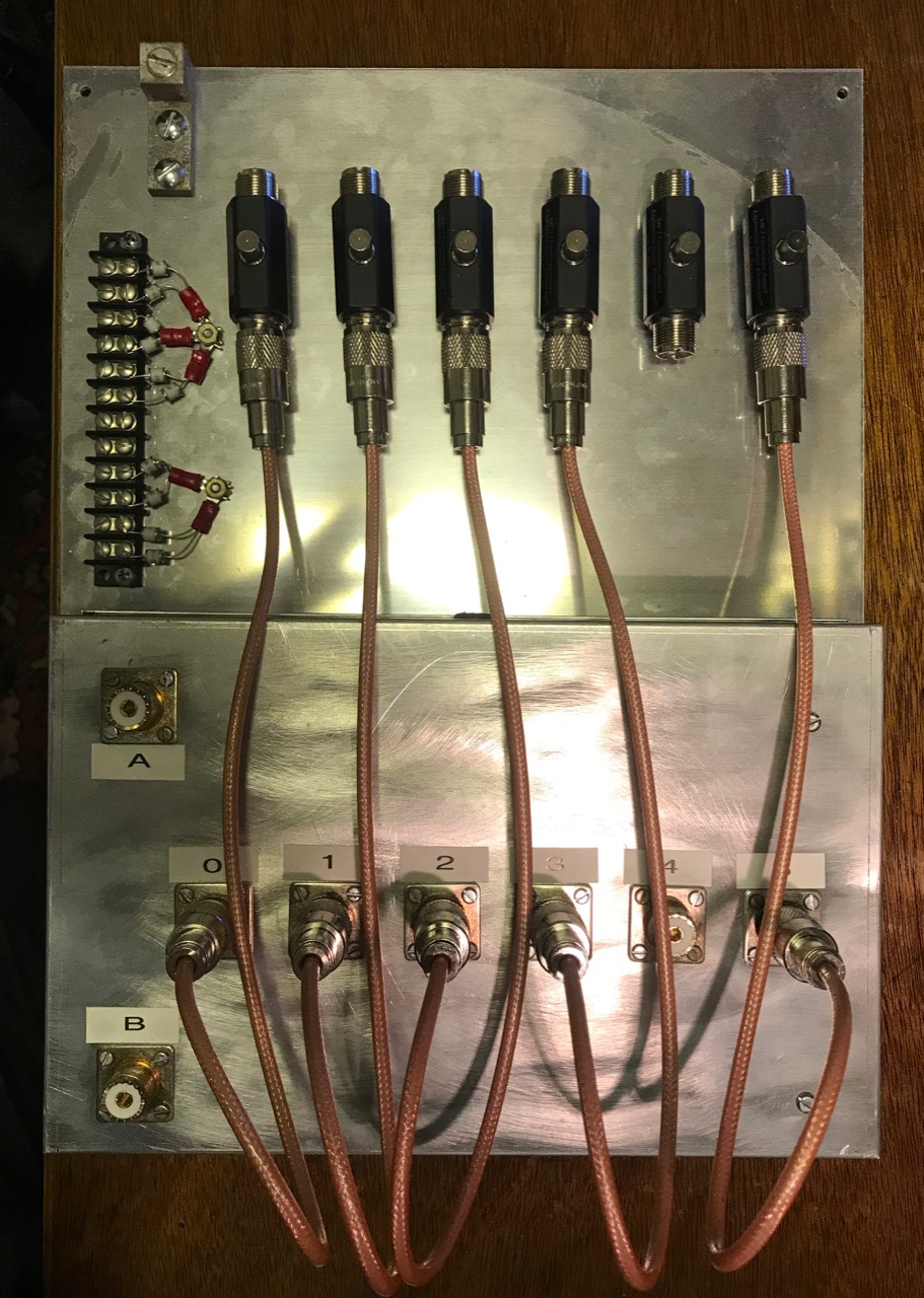
As radio amateurs, taking proper precautions against lightning and electrical surges can be a difficult and expensive proposition. We often neglect them and rely on luck.
After reading Bonding and Grounding for the Radio Amateur, I decided it was worth the investment. I already had all ground connections - house, tower, station - bonded. What was missing was bonding the antenna connections to the ground as they entered the house. I needed a Single-Point Ground panel.
A Single-Point Ground is a metal panel or box providing a common bonding point for all cables as they enter a building. This metal is connected to the external ground rods, which are all bonded together. The idea is to bond the cables connected together, so that lightning or surge potentials all rise and fall together. Without a potential difference, damaging currents cannot flow.
SPG panel ready to mount on basement wall
I cut a 0.090" Aluminum panel 12" by 16" and mounted the KK1L antenna switch to the bottom edge. I added lightning arrestors for the antenna coaxial cables, plus a barrier strip holding gas discharge tubes for the rotator and shunt antenna control cables.
I chose MFJ-272 lightning arrestors. I needed six of these, and the MFJ units were about $40 each. The Alpha Delta and Polyphaser units were more expensive. The arrestors are mounted to the panel with a single large screw, supplied with the arrestor.
Short coaxial jumpers connect the arresters to the KK1L switch. I made these out of 18 inches of RG-400 coax using new Amphenol UHF connectors and a UG-175 adapter. RG-400 is doubly-shielded, eliminating the potential for any coupling between the jumpers. (Notice I didn't quite have enough RG-400 for all six jumpers, so there are only five at the moment. I'll have to purchase more)
The panel mounts on the basement wall where the cables enter the house through a 4 inch PVC pipe. A grounding block connects a short piece of copper wire to an eight foot ground rod on the outside. The ground connection is also bonded to the perimeter ground wire between the house, tower and station grounds using a split bolt.
I had a bit of trouble with the coax running from the A and B ports of the KK1L to the operating desk. Since the coax to the antennas ended at the basement wall, I trimmed some coax from the antenna feed lines. To get the right length, I pulled the feed lines outside, then trimmed them from the far end. Simple, eh? Except the first one looped around and got stuck, and the cut piece ended up being about five feet too short.
The next feed line was a newer run of Davis Buryflex. I ran it to the A3S/A743, and then cut the right length. For some reason, I had problems with the connectors on both ends, but once they were redone, the cable worked as expected. For a short while, I thought the cable itself might be defective.
To do these tests, I made good use of my RigExpert AA-55 Zoom. Which of two pieces of old coax is any good? The cable loss test is quick and give one real numbers to compare. You just need to test the coax both open and shorted.
With the SPG installed, the next step is to automate the switching of the KK1L.
Cable management trays added to back of desktop selves.
Now that my station desktop is on wheels and has a set of nice shelves, I wondered might be done about the rats nest of wires hanging down from the back of the desk. Some kind of cable management system was needed.
These systems can be expensive. I found a solution on Amazon.com that worked pretty well. It is a kit of eight cable raceway trays about 15" long, 1.5" wide and just under 1" tall. All for just about $20.
These worked well with my desktop shelves. Three cable trays fit neatly on the back of the shelves just under the copper pipe ground bus bar. I mounted them using three short wood screws on each tray.
The tops of the trays either slide or snap off. The fingers on the sides are easily displaced to insert wires of just about any size. In some cases, cables are routed in the trays from one end of the shelves to the other.
From the picture, there are still a lot of wires, but it is neater and more manageable than before. Many of those are antenna coax or power connections. The antenna coax will be moving to the back wall of the basement once the Single-Point Ground (SPG) panel is in place.
I also improved the bonding between units. I'm using 1/2" tinned copper braid, a fork lug and a cable clamp around the 1/2" copper tube grounding bus. This creates a low-impedance connection between the equipment and the station ground. In a few cases, I had to drill a hole and add some #6 screws and nuts to make the connection.
The best part is, I still have five left-over cable management trays to use elsewhere.