Normal view

There are new articles available, click to refresh the page.
Before yesterdayKA7OEI's blog

Exploring the NDK 9200Q7 10 MHz OCXO (Oven-controlled Crystal Oscillator)

By: Unknown
29 December 2022 at 00:22

Figure 1:
The NDK 9200Q7 OCXO.  This unit, pulled from
used equipment, is slightly "shop-worn" but still
serviceable.  The multi-turn tuning potentiometer
is accessible via the hole at the lower-left.
Click on the image for a larger version
The NDK 9200Q7 (pictured) is an OCXO (Oven-Controlled Crystal Oscillator) that occasionally appears on EvilBay or surplus sites.  While not quite as good a performer as the Isotemp 134-10 (see the 17 October, 2017 Blog entry, "A 10 MHz OCXO" - Link) it's been used for a few projects requiring good frequency stability, including:

  • The 146.620 Simulcast repeater system.  One of these is used at each transmitter site, which are held at 4 Hz apart to eliminated "standing nulls" - and they have stayed put in frequency for over a decade. (This system is described in a series of previous blog entries starting with  "Two Repeaters, One System - Part 1" - Link).
  • 10 GHz transverter frequency reference.  One of the local amateurs used one of these units to hold his 10 GHz frequency stable and it did so fairly well, easily keeping it within a  hundred Hz or so of other stations:  This was good enough to allow him to be easily found and tuned in, even when signals were weak.

At least some of these units were pulled from scrapped VSAT (Very Small Aperture SATellite) terminals so they were designed for both stability and the ability to be electronically tuned to "dial in" the frequency precisely.

Testing and experience shows that given 10-15 minutes to thermally stabilize, these units are perfectly capable of holding the frequency to better than 1 part in 108 - or about 1 Hz at 100 MHz - and since any of these units that you are likely to find about are likely to be 25-30 years old, the intrinsic aging of the quartz crystal itself is going to be well along its asymptotic curve to zero.

Figure 2:
The bottom of the OCXO, annotated to show the various
connections.
Click on the image for a larger version.

Using this device

In its original application, this device was powered from a 12-15 volt supply, but if you were to apply power and give it 5-15 minutes to warm up, you would probably be disappointed in its accuracy as it would not have any sort of external tuning input to get it anywhere close to its intended frequency.

Because of the need for it to be electrically tuned, this device is actually a VCXO (Voltage-Controlled Crystal Oscillator) as well and as such, it has a "Tune" pin, identified in Figure 2.  Nominally, the tuning voltage was probably between 0 and 10 volts, but unless a voltage is applied, this pin will naturally drift close to zero voltage, the result being that at 10 MHz, it may be a dozen or two Hz low in frequency.

Adding a resistor

The easiest "fix" for this - to make it operate "stand-alone" - is to apply a voltage on the pin.  If your plans include locking this to an external source - such as making your own GPSDO (GPS Disciplined Oscillator) then one simply need apply this tuning voltage from a DAC (Digital-to-Analog Converter) or filtered PWM output, but if you wish to use this oscillator in a stand-alone configuration - or even as an externally-tuned oscillator, a bit of modification is in order.

Figure 3:
This shows the 10k resistor added between the internal 5 volt
source and the "TUNE" pin to allow "standalone" operation.
Click on the image for a larger version.
The OCXO may be disassembled easily by removing the small screw on each side and carefully un-sticking the circuit board from the insulation inside.  Once this is done, you'll see that there are two boards:  The one on the top is part of the control board for the heater/oven while the bottom houses some of the oscillator components.

Contained within the OCXO is a 78L05 five-volt regulator which is used to provide a voltage reference for the oven and also likely used as a stable source of power for the oscillator - and we can use this to our advantage rather than need to regulate an external source which, itself, is going to be prone to thermal changes.

Figure 3 shows the addition of a single 10k resistor on the top board, connecting the "TUNE" pin to the output of this 5 volt regulator.  By adding this resistor, the TUNE pin allows one to use this OCXO in a "standalone" configuration with no connection to the "TUNE" pin as it is is automatically biased to a temperature-stable (after warm-up) internal voltage reference and can then be used as-is as a good 10 MHz reference, using the onboard multi-turn potentiometer to precisely set the frequency of operation.

Figure 4:
More pictures from inside the OCXO
Click on the image for a larger version.
Another advantage of adding the internal 10k resistor is that it's easy to reduce the TUNE sensitivity from an external voltage:  This value isn't critical, with anything from 1k to 100k likely being usable.  Testing shows that by itself, the oscillator is quite table and varying the TUNE voltage will adjust it by well over 10 Hz above and below 10 MHz.

The inclusion of the 10k internal resistor may also be of benefit.  In many cases, having a much narrower electronic tuning range than this will suffice so a resistor of 100k (or greater) can be used in series with the TUNE pin, between it and an external tuning voltage, acting as a voltage divider.  Doing this will reduce the tuning range and it can also improve overall stability since much of the tuning voltage will be based on the oscillator's already-stable 5 volt internal source.  The stability of the OCXO itself is such that even with a 10-ish:1 reduced tuning range due to a series 100k resistor, there is still far more external adjustment range than really necessary to tune the OCXO and handle a wide range of external temperatures.

The actual value of the added internal resistor is unimportant and could be selected for the desired tuning/voltage ratio based on the external series tuning resistor and the impedance of the tuning voltage.

When reassembling the OCXO, take care that the insulation inside the can is as it was at the time of disassembly to maximize thermal stability and, of course, be sure that the hole in the can lines up with the multi-turn potentiometer!

Operating conditions

Figure 5:
Even more pictures from inside the OCXO.
Click on the image for a larger version.
The "official" specifications of this OCXO are unknown, but long-term use has shown that it will operate nicely from 12-15 volts - and it will even operate from a 10 volt supply, although the reduced heater power at 10 volts causes warm-up to take longer and there may not be sufficient thermal input for the oven to maintain temperature at extremely low (<15F, <-9C) temperatures unless extra insulation is added (e.g. foam around the metal case.)

It is recommended that if one uses it stand-alone, the voltage source for this device be regulated:  While the on-board 5 volt regulator provides a stable reference without regard to the supply voltage, the amount of thermal input from the oven will change with voltage:  More power and faster heating at higher voltage.  While you might think that this wouldn't affect a closed-loop system, it actually does owing to internal thermal resistance and the fact that due to loss to the environment, there will always be a thermal gradient between the heater, the temperature-sensitive circuitry, and the outside world - and changing the operating voltage and thus the amount of heater power will subtly affect the frequency.

Finally, this oscillator - like any quartz crystal oscillator that you are likely to find - is slightly affected by gravity:  Changing orientation (e.g. turning sideways, upside-down, etc.) of this oscillator affects its absolute frequency by a few parts in 10E-8, so if you are interested in the absolute accuracy and stability, it's best to do the fine-tuning adjustment with it oriented in the same way that it will be used and keep it in that orientation.

* * * * * * * * *

This page stolen from ka7oei.blogspot.com

[End]


An LCD Retrofit and color display for the Schlumberger SI 4031 Communications Test Set

By: Unknown
2 December 2022 at 21:40

Figure 1: 
The front panel and original green monochrome screen
of the 4031.  A close look shows the "blistering" on the
screen protectors due to delamination, making the
display more difficult to read.
Click on the image for a larger version.
The Schlumberger SI 4031 is a early-mid 1990s vintage communications test set (a.k.a. "Service Monitor") - a device that is designed to test both receivers and transmitters used in the telecommunications industry.  The 4031's frequency range is 400 kHz to 999.9999 MHz making it useful as a general-purpose piece of test equipment, particularly for the testing of amateur radio gear.
Some of its built-in functions include wattmeter, signal generator with modulator for AM, FM and phase-modulated radios, spectrum analyzer, tracking generator and oscilloscope to mention but a few.

As you would expect from a device from the 1990s, the original display used a CRT (Cathode Ray Tube) based monitor operating at something "close" to PAL horizontal and vertical scan rates.  While the CRT monitor in this unit is still in reasonable shape - aside from requiring a "re-cap" (e.g. replacement of electrolytic capacitors) I decided to take on the challenge of putting a more "modern" LCD-type display in it - perhaps taking advantage of a minor savings in both weight and power consumption.

This requires no electrical modification of the 4031 itself and only minor mechanical changes to mount the LCD panel and its related hardware.  (This may also work for the 4032, a version of this unit that covers up to 2 GHz - see below for comments.)

Is it "PAL"

While the pedants would say that a monochrome-only signal cannot be PAL, the reference is, instead, to the horizontal and vertical scan rates of 15.625 kHz and 50 Hz, respectively which are close to those found in the PAL system used in Europe.  As is typical for pieces of non-consumer gear and test equipment, the horizontal and vertical synchronization signals and the video are brought out independently of each other, each being represented as a TTL signal.

Figure 2:
The horizontal sync pulse train showing 25%
D.C. pulses at 15.625 kHz, TTL level.
Click on the image for a larger version.
The video display generator of the 4031 is interesting in that it uses a UPD7220A graphics controller to facilitate interaction with the CPU (e.g. access memory, produce characters, etc.) but two separate display RAMs (8k x 16 bits) with one being used for access by the UPD7220A and the other, copied from the first during the vertical interval, for pixel read-out - the latter function being done with a combination of "glue logic" and programmable logic devices.

The forgiving nature of the CRT monitor

One nice feature of a CRT monitor is that it can be quite forgiving of deviations from standard video applied to it.  Many - but not all - all-in-one sync decoder chips used in CRT monitors are happy with taking horizontal and vertical signals that are "close" to some standard - but not exact - and lock onto it satisfactorily.  Such is the case with the 4031:  While there are separate horizontal and vertical synchronization signals, neither is quite standard, but it's "close" enough for the old monitor.

Figure 3: 
The vertical sync, showing a 10% duty cycle
pulse at about 50 Hz.
Click on the image for a larger version.

For example, the horizontal synchronization signal is simply an uninterrupted 25% duty cycle pulse train occurring at the horizontal sweep rate of about 15.625 kHz (e.g. 16uSec long) while the vertical synchronization is a 50.08 Hz 10% duty cycle (e.g. 2 msec long) pulse train.  Unlike sync signals found in other applications, the horizontal signal does not contain any sort of blanking (suppression of pulses) during the vertical interval.

Within the 4031's original CRT monitor, the horizontal and vertical synchronization signals are handled completely separately (by a TDA2593 and TDA1170, respectively) so the fact that they are non-standard is irrelevant.

Unfortunately, any modern LCD display device that is expecting a PAL-like signal (in terms of timing) isn't likely to be happy with separate, non-standard synchronization inputs.

Initial attempts:

Initially, I was hoping that an off-the-shelf LCD monitor display like the 7", 4:3 aspect CLAA070MA0ACW with a driver board could be made to work with these signals with no other hardware, but my work was thwarted by the fact that its VGA input - which might handle separate horizontal and vertical sync signals - would not function at PAL video rates - only VGA rates, which have roughly twice the horizontal and vertical frequencies.  While it may have been possible to modify the firmware on this board and re-flash it with one of the "customized" versions found in various corners of the Internet, I chose not to do this.

I then attempted to make a simple analog sync combiner circuit and apply the signal to the composite video input, but found this to be unstable - plus there was the fact that the video display board itself did not have the capability of setting the horizontal and vertical size to fully-fill the screen to the edges, something desirable to make the active screen area fully-fit the window on the front and also align with the buttons along the bottom of the screen.

After a bit more research, I decided to get a GBS-8200 video converter board (Version 4.0), a relatively inexpensive digitizing board designed to convert the myriad of video formats from CRT-based arcade video games and computer inputs to VGA which would then be inputted to a standard monitor and the CLAA070MA0ACW display driver board.  As such, I presumed that it would be far more forgiving to variations from standard video signaling - and I was, fortunately, correct

Sync (re)processor:

While I was originally hopeful that I could simply apply the horizontal and vertical sync inputs to the GBS-8200, the non-standard sync timing (pulse width, lack of a gap of horizontal sync pulses during the vertical interval) did not produce stable results, so a simple circuit had to be devised to modify the sync signal:  This basic circuit is shown below.

Figure 4:
Diagram of the sync processor itself.
This circuit will produce a sync to which the GBS-8200 board can lock.  The single video output
is connected to the RGB input of the GBS-8200 to produce a monochrome (single color)
display as seen in Figure 6.
Click on the image for a larger version.

This circuit works as follows:
 
The horizontal and vertical sync pulses are input to and buffered by sections of a 74HC14, Schmidt-trigger inverters which server to "clean up" the input signals as necessary.  An inverted version of the vertical sync pulse holds U3, a 4017 counter in reset until a vertical interval occurs.

Figure 5:
The circuit in Figure 4 built
on a prototyping board, the
results seen in Figure 6.
Click for a larger image.

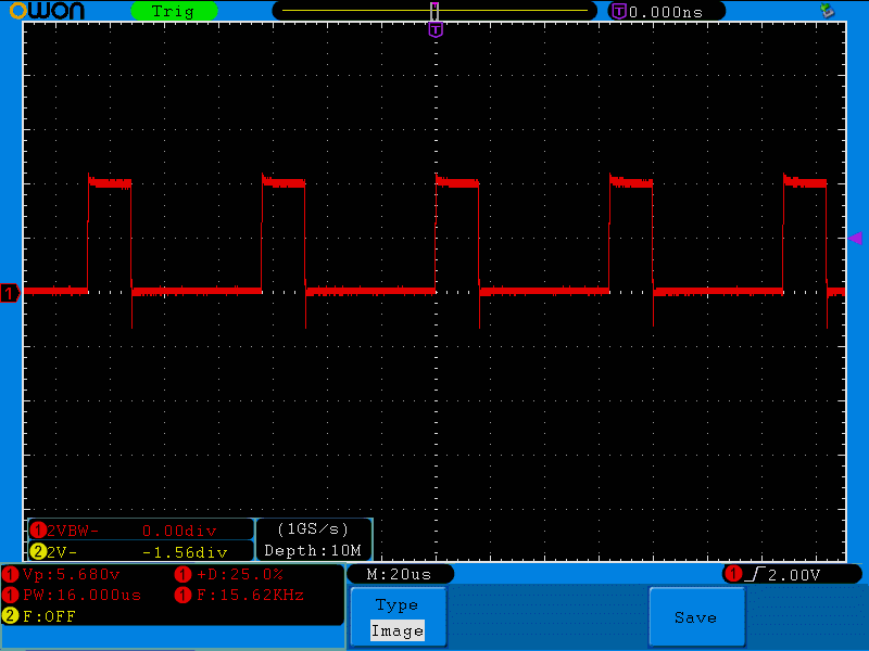
During the vertical pulse U3, the counter, is clocked by the horizontal sync pulses and on the 5th count, the timer is stopped, setting the input of U2b, a 4011 NAND gate wired as a simple inverter, high.  U2d is used to "gate" the output of the counter - being only active only when the timer has stopped at the 5th count and during the vertical interval meaning that its output goes high only when the timer is actually counting - not while it's stopped at its terminal count or held in reset. The output of this gate is combined with a "re-inverted" copy of the vertical sync to produce a new version of the vertical sync that is about 225 microseconds long rather than the original 2 milliseconds as depicted in Figure 7 (below).

FWIW, I used the 4011 NAND gate because I found a rail of them in my parts bin - but I couldn't find any 74HC00s at the time which would have worked fine, albeit with a different pin-out.  Similarly, either CMOS CD4017 or 74HC4017 counter would have been fine as well considering the low frequencies present.  I would, however, recommend using only the 74HC14 (or 74HCT14) as it's plenty fast for the video data and it has fairly "strong" outputs (e.g. source/sink currents) as compared to the older and slower CD4069 or 74C14 hex Schmidt inverter.

Note that while it would theoretically be possible to use a one-shot analog timer to generate a new, shorter pulse, doing so would result in visible jitter of the video signal (I tried - it did!) as that timing would neither be consistent or its length precisely synchronous with the horizontal timing:  The use of the horizontal sync to "re-time" the duration of this new vertical pulse assures that the timing of the new pulse is synchronous with both sets of pulses and completely jitter-free.

This new, re-timed vertical sync pulse is then applied to U2a which gates it with the horizontal sync:  The output is then inverted by U1c to produce a composite sync signal (see Figure 7, below) that, while not exactly up to PAL standards, is "close enough" for the GBA-8200 video converter - configured for "RGBS" mode - to be happy.

Elsewhere in the diagram may be seen inverter sections U1d-U1f:  These are configured as buffers to condition the TTL video input and provide a drive signal to the video input of the GBA-8200.

Suitable for a monochrome image!

The circuit in Figure 4 is sufficient, by itself, to drive the GBS-8200 and produce a stable VGA version of the 4031's video signal.

Figure 6:
The monochrome output from the GBS-8200 board using the
sync processor seen in figures 4 and 5 via an external monitor.
Click on the image for a larger version.
The "VID_OUT" signal may be connected to the Red, Green and Blue video inputs of the GBS-8200 and the input potentiometers adjusted for a single color:  White will result if the individual channels' gains are set equally, but green, yellow or any other color is possible by adjustment of these controls.

Figure 6 shows the result of that:  The VGA output from the GBS-8200 was connected to an old 4:3 computer monitor that I had kicking around, producing a beautiful, stable, monochrome signal.

Full-color output from the 4031

The SI 4031's video output is a single TTL signal, meaning that there is not even any brightness information, making it capable of monochrome only.  Fortunately, it is possible to simulate context-sensitive color screens with the addition of a bit of extra circuitry and firmware as described below.

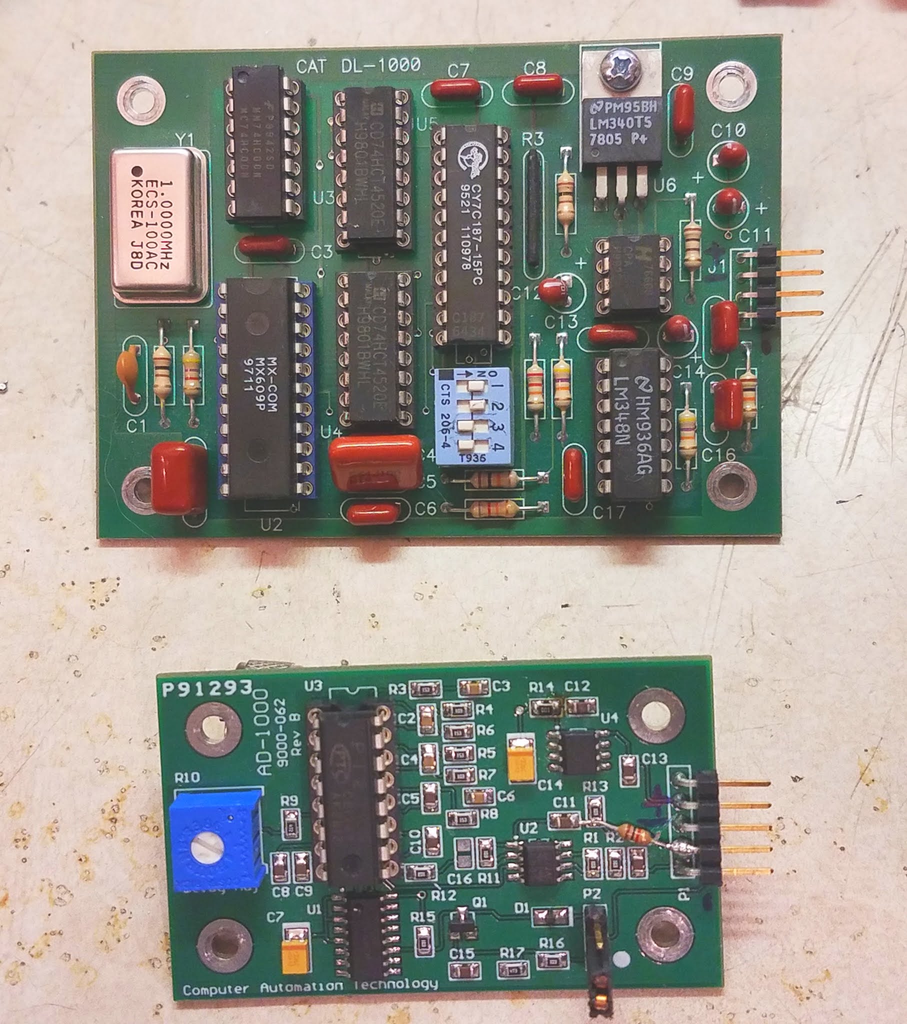
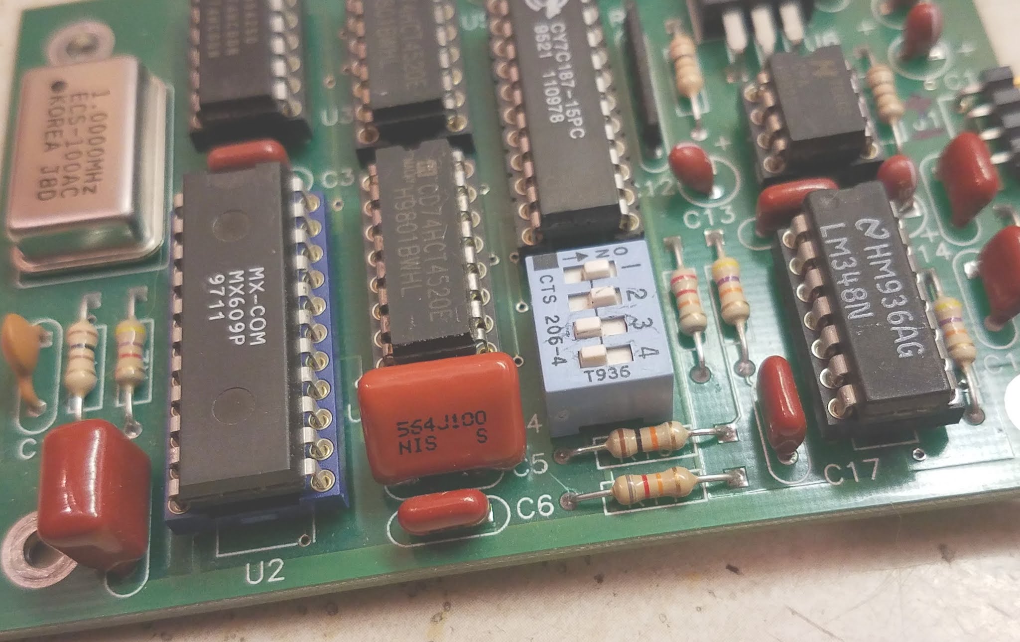
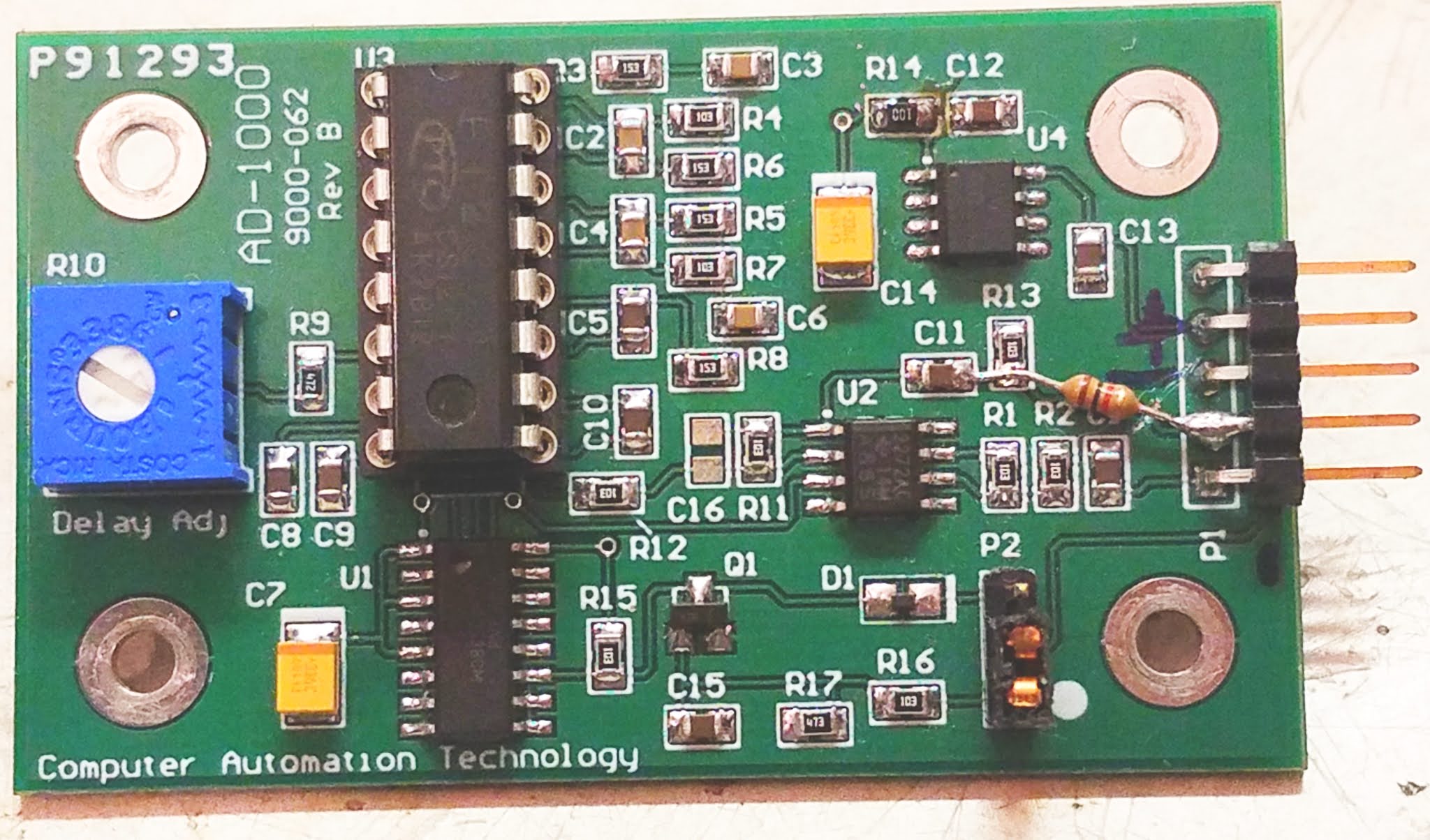
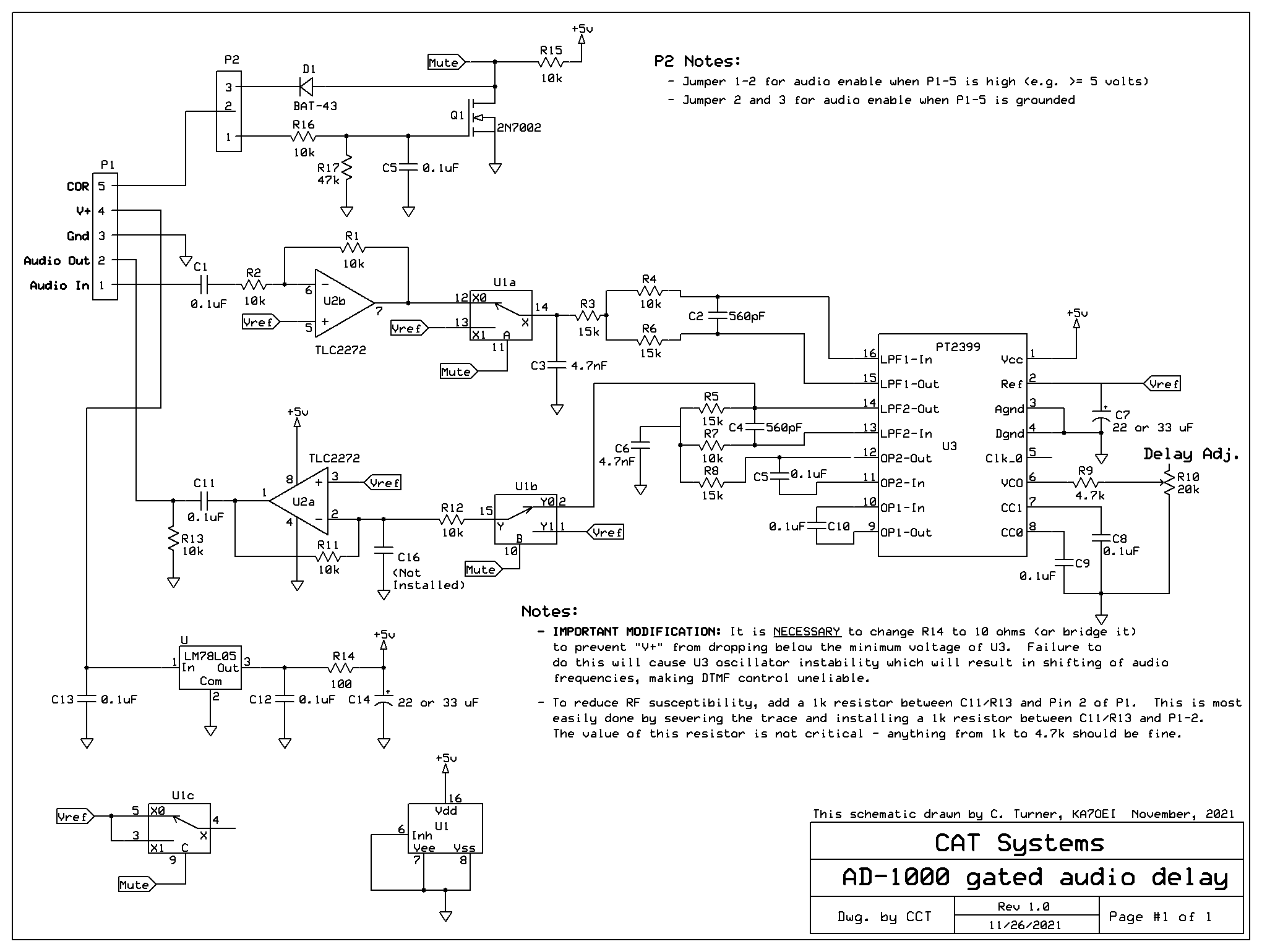
The portion of this circuit used for processing the sync pulses is based on that shown in Figure 4:  A few reassignments of pins were done in the sync re-timer, but the circuit/function is the same.  What is different is the addition of U5, a 74HC4066 quad analog switch and U6, a PIC16F88 microcontroller, and a few other components.

How it works:

The video signal is buffered by U1d-U1f and applied to R1, a 200 ohm potentiometer, the wiper of which is applied to Q1, a unity-gain follower to buffer the somewhat high-impedance video from R1 to something with a source impedance of a few ohms and, more important, constant output with varying load.  The "bottom" end of R1 is connected to U5c, on section of the 74HC4066 which, if enabled, will shunt some of the video signal to ground, reducing its intensity, adjustable via R1.  Via diode D1, this line is also connected to a pin of the microcontroller - the "MARK" pin - more on this later.

Figure 7:
Top (red) trace: The composite sync from the
circuit of Figures 4 & 8.  Bottom (yellow) trace:
The original vertical sync pulse  for comparison.
Click on the image for a larger version

The output of Q1 is then applied to U5a, U5b and U5d via 100 ohm resistors.  These analog switches will selectively pass the video to the Red, Green or Blue channels of the monitor, depending on microcontroller control.  At the outputs of each of these switches may be found a resistor and diode in series (e.g. D2/R6) and these are connected to output pins of the microcontroller:  If these pins are driven low by the microcontroller, the diode drop and series resistance of the 33 ohm resistor (e.g. R6) and the 100 ohm resistor (e.g. R3) and the output transistor of the microcontroller will shunt some of the voltage and reduce the amplitude on that channel to provide a means of brightness control, increasing the color palette.

I'd originally intended to place emitter-follower video drivers (e.g. the circuit of Q1 in Figure 8) on each of the R, G, and B outputs, but the very short lead length to the input of the GBS-8200 (e.g. no visible signal reflections) - and the ability to adjust the RGB input gain via its three potentiometers - eliminated this requirement as additional losses through the analog switches and other components could be easily compensated.

Figure 8:
Added to the sync processor of Figure 4, above, is a PIC16F88 used to analyze the video from the 4031
and "colorize" the resulting image. 
See the text for information as to how this works.
Click on the image for a larger version.

With the combination of the three 4066 gates, the "!BRITE" pin, and the three "dim" pins (e.g. "!R_DIM", "!G_DIM" and "!B_DIM") over two dozen distinctly different colors and brightness levels may be generated under processor control.

The magic of the microcontroller

U6, a PIC16F88 microcontroller, is clocked at 20 MHz, its fastest rated speed.  Because its job is to operate the four switches comprising U5 - and the three "dim" pins on the video lines - it must "know" a bit about the video signal from the 4031:

  • The "!V_SYNC" pin gets a conditioned sample of vertical sync from the output of U1a:  It is via this signal that the U6 "knows" when the scan restarts at line one.
  • The "!H_SYNC" signal from the output of U1b is applied to pin RB0, which is configured to trigger an interrupt on the falling edge (the beginning) of the horizontal sync.
  • The "!VID" signal is applied to pin RA4, which is the input of Timer 0 within the microcontroller:  This is used to analyze the content of lines of video to determine the specific content as the timer is able to "count" the number of times that the video goes from low to high on these scan lines -  In other words, a sort of "pixel count".

In operation, the start of each horizontal sync pulse triggers an interrupt in the microcontroller.  If this coincides with the start of the vertical interval, the line count is restarted.

Video content analysis:

Figure 9:
Mounted inside the 4031, the sync processor board is on the
far left, the six pins of the ICSP (In Circuit Serial
Programming) connector being easily accessed.  The buttons
and controls for the other two boards are also accessible.
Click on the image for a larger version.

Visual inspection of each of the screens on the 4031 will reveal that they contain unique attributes.  Most obvious is the title of the screen located near the top, but other content may be present midway down the screen - or very near the bottom - which may be used to reliably identify exactly which screen is being displayed, having determined the "pixel count" for certain lines on each of these screens beforehand.

For each subsequent horizontal sync pulse and corresponding interrupt, the count contained within hardware timer 0 is read - and the timer is immediately reset.  For a number of specific scan lines, their unique counts are stored in RAM.

Attention to detail is required!

Determining the pixel count consistently requires a bit of care in the coding.  As mentioned, this count is based on an interrupt-driven routine that reads the content of hardware timer 0 - but this also means that the code must be written in a way that guarantees that the time between the start of the horizontal sync pulse (and subsequent entry into the interrupt service routine) and the read and reset of timer 0 is as consistent as possible, considering the asynchronicity of the timing of this interrupt and the CPU clock.

What this implies is that the reading this timer and its resetting must not only be done in an interrupt, but that it also be the first thing done within the interrupt function prior to any other actions, particularly any conditional instructions that could cause this timing to vary, resulting in inconsistent pixel counts - something that would preclude the use of anything other than a quickly-responding interrupt.  Another implication is that this interrupt may be the only interrupt that is enabled as preemption by another one would surely disrupt our timing.

Immediately following this action is the setting of the color and brightness attributes by ANDing a copy of the current content port/pin registers to remove the brightness/color bits and then ORing that data with the pre-calculated color/brightness bit mask data into those same registers so that any changes in these attributes occur to the left of the visible pixels in the scan line.

A limitation of this hardware/software is that it is likely not possible to satisfactorily set different colors horizontally, along a scan line - it is possible only to change the color of complete scan lines:  To do this would, at a minimum, require extremely precise timing within the interrupt service routine, adding complexity to the code - and it's not certain that satisfactory results would even be possible.   To do it "properly" would certainly require more complicated hardware - possibly including the regeneration of another clock from the horizontal pixel rate - but doing this would be complicated by the fact that the pixel read-out rate is asynchronous with the sync as noted later.

Using the pixel counts:

At the beginning of the vertical interval, outside any interrupts, the previously-determined counts of low-to-high transitions is analyzed via a series of conditional statements and a variable is set indicating the operating "mode" of the 4031.  This "mode" information is then applied to another look-up table to determine the color to be used for that screen.

One complication is that like other analog video, that coming from the 4031 is interlaced meaning that for certain scan lines - particularly those with diagonal elements - that the pixel count may vary for a given scan line.  Unlike "true" video, the sync pulses from the 4031 contain no obvious timing offset (e.g. "serrations" in the sync) to offset by half a line or identify the specific video field, but with an analog monitor, this wasn't really much of an issue as it would simply paint a line on the screen in "about" the right place, anyway.

For most screens, simply looking at pixel counts of between four and six different lines - most of them on lines from 4 to 15 - was enough to uniquely identify a screen, but others - particularly the "Zoom" screens - sometimes require even a greater number of pixel counts and other techniques to reliably and uniquely identify the screen being displayed.

In particular, differentiating between the "SINAD" and "RMS-FLT" Zoom screens was problematic as both resulted in the same pixel counts for all of the lines usable for unique identification:  The only way to detect the difference was due to the fact that for some lines, the pixel count for the "SINAD" screen would vary due to the aforementioned video field differences - or possibly due to interaction between the asynchronicity of the pixel clock, the CPU clock, and the way counts are registered on a counter input without hardware prescaling.  It was the fact that the count of the SINAD screen varied that allowed it to be reliably differentiated from the "RMS-FLT" screen, which had a very consistent pixel count.

Coloration of the screen:

Many screens on the 4031 have different sections.  For many screens, the upper section contains the configured parameters (e.g. frequency, RF signal level, etc.) while the lower portion of the screen shows the measured values or an oscilloscope display:  Simply by knowing which screen type is being displayed and the current line number, those sections can be colored differently from other portions.

Deciding what color to make what is a purely aesthetic choice, so I did what I thought looked good.  Because about two-dozen different colors are possible, I chose the brightest colors for the most commonly-used screen segments, setting these colors by the function to which they were related.

Finally, all screens have, along the bottom, a set of labels for the buttons below the bottom of the screen:  These may be colored separately as well - and I chose gray (a.k.a. "dim white").

Analyzing the video to determine "pixel counts":

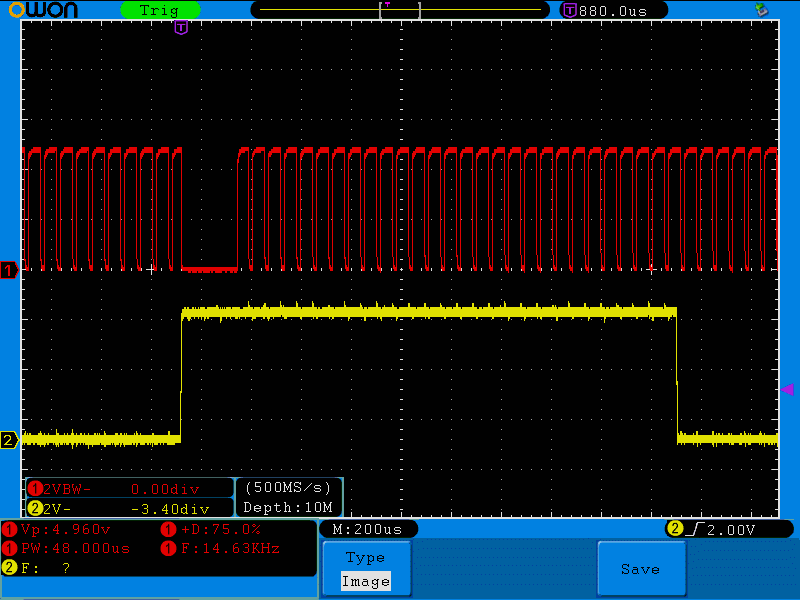
When writing the firmware, a few simple tools were included, notably some variables, hard coded at compile time, that would display the pixel counts.  If, for example, one needed to determine the pixel count for line #14, the pixel count display variable would then be loaded with the pixel count for line 14.  For example, the oscilloscope screen capture shows a pixel count capture:  The left-most pulse is 4 units long followed by a single-unit pulse (meaning "10") followed by a 2 unit long pulse with three more pulses - for a pixel count of 13.

Figure 10:
An example of the "pixel" count:  The 4-unit
wide pulse followed by one pulse represents 10
and the 2-unit wide pulse followed by 3 pulses
represent a pixel count of 13 on the selected line.
Click on the image for a larger version.

Another variable may be set to visually identify which scan line is being counted.  When the scan line being counted occurred, the "MARK" pin would be set high causing an on-screen indication of which line was being inspected, offering a "sanity check" and a visual reference to know which line, exactly, was being checked.

During the vertical interval, pin "RB3" would then be strobed with a series of pulses to indicate the pixel count - a "long" pulse lasting four CPU cycles followed by pulses of 1 CPU cycle, each to indicate the "tens" digit (if any) and a shorter pulse of two CPU cycles followed by the requisite number of 1 CPU-cycle pulses to indicate the "ones" digits. 

Using an oscilloscope triggered on the signal on RB3 (pin 9) these pulses could be read visually on the oscilloscope and by switching between the different screens on the 4031, the "pixel count" of this line for the various screens could be determined:  Repeating this for several different scan lines allow unique identification of all screens.  In the event that there is false detection of a mode, this "pixel count" output could also be configured to show the number of the current modes (in a "#define" statement) when they are detected to aid in debugging.

Comments:

In producing this firmware, I have only one version of the 4031 (with Duplex option) available to me.  Different versions of the 4031 - and the 4032 - may have "other" screens not included in the analysis, or slightly different layout/labeling that will foil the analysis of the scan line.
The way the firmware doing the screen analysis is written, if the scan line analysis doesn't find a match to what it already "knows" about it will cause that screen's text to be displayed in the default color of white.

At present this "scan line analysis" can only be done by setting certain variables in the source code and recompiling - but this was made easier by the inclusion of the "ICSP" connector (noted on the diagram in Figure 8 and visible in Figure 9) to allow in-circuit programming, while the unit is operating.  In theory, it may be possible to come up with some sort of user-interactive means of setting individual screens' colors which could be used to set the colors on screens of different firmware versions or with features that I don't have in my 4031, but this would require significantly more work on the firmware.

Figure 11:
The 4031 with the retrofit LCD operational.
This isn't a perfect photo because it's very difficult to take
a picture of an operational electronic display!
Click on the image for a larger version.

Color mode selection:

With the lack of the CRT monitor, there is no need for an "intensity" control, but rather than leave a hole in the front panel a momentary switch was fitted at this position.  Connected between ground and pin RB7, using the processor's internal pull-up resistor, this switch is monitored for both "short" and "long" button presses.

A "short" press (less than 1/2 second) toggles between "bright" and "dim" using the same color scheme, but a "long" press (1.5-2 seconds) changes to the next the color mode.  At the time of this writing, the color modes are:

  • Full-color screens.  The screens are colored according to mode and context as described above.
  • Green.  All components of the screen are green.
  • Yellow.  Like above, but yellow.
  • Cyan.  Like above, but cyan.
  • Pink.  Like above, but pink
  • White.  Like above, but white

In some instances (e.g. high ambient light) selecting a specific color (green or yellow) may improve readability of the screen.  These settings selected by the switch are saved in EEPROM (10 seconds after the mode was last changed) so that they are retained following a power-cycle.

* * * * * * *

The hardware

Several bits of hardware are required to do this conversion and if you are of the ilk to build your own circuits, nothing is particularly difficult.  Personally, I spent at least as much time making brackets and pieces and mounting the hardware in 4031 as I did writing the firmware.

Sync processor:

At a minimum, the "simple" sync processor mentioned above (Figure 4) is required to provide a synchronization pulse that is recognizable by the converter board.  If one doesn't wish to have different color modes available, this is certainly an option.

Having said that, the "colorized" 4031 afforded by the circuit described in Figure 8 is quite nice - perhaps a bit of an extravagance.  If the 4031 were originally equipped with a color monitor, I can imagine it looking something like the the images in the "Gallery" section of this article, below.

"Where's the PCB?"

As can be seen in Figures 9 and 21 the circuit in Figure 8 was constructed on glass-epoxy perfboard - the type with individual rings around each hole:  I did not design or lay out a PCB as I could build 2 or 3 of these in just the time that it would take to do so - and that wouldn't include the revisions or debugging.

Constructed in this way, I could easily try out new ideas - one of which was the later addition of the "D_RED", "D_GREEN" and "D_BLUE" brightness controls which were included on a whim fairly late in testing:  This was trivial to test and add to the perfboard, but I would certainly have not bothered with this significant enhancement if I'd already "frozen" the design in the embodiment of a PC board.

Unless I feel inclined to build a bunch more of these, I'm not likely to design a PCB, but if YOU do, let me know so that it may be shared. 
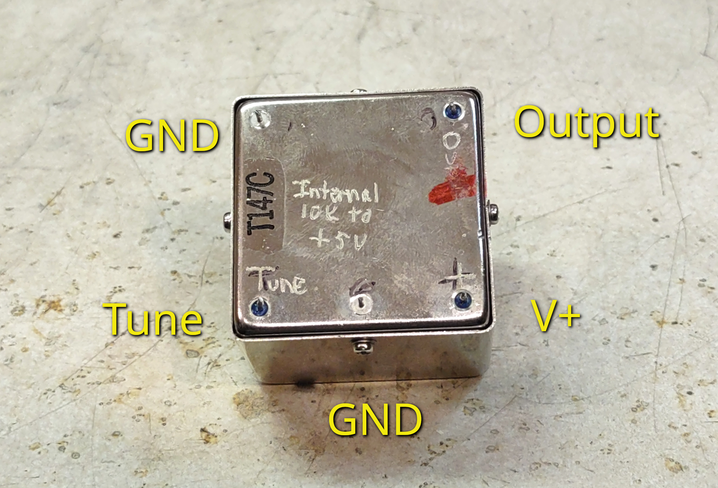
GBS-8200:

Figure 12:
The GBS-8200 video converter board.  This is "V4.0" of
the GBS-8200 which includes an on-board voltage regulator
allowing it to run from 5-12 volts.
Click on the image for a larger version.

There appear to be several versions of the GBS-8200 around - possibly from different manufacturers and some of these are designed to be operated from a 5 volt supply ONLY, but many have on-board voltage converters, allowing them to be operated from 5 to 12 volts:  The version that I have is the "V4.0" board with a "5-12 volt" input which eliminates the need for yet another voltage conversion step.  If you look carefully at the photo of the GBS-8200, the inductor for the buck converter is visible near the upper right-hand corner of the board, between the power connector the white video-out connector marked "P12" - but the silkscreened "DC 5V-12V" is also a big give-away!

This board, readily available via EvilBay and Amazon for well under US$40, is specifically designed to take a wide variety of RGB video formats - typically from 70s-90s video games and computers - and convert them to VGA format.  There are several connectors for video input seen along the bottom edge of the photo:  The three phono plugs for component video, an input on a VGA connector, and next to the VGA connector, two white headers for cable:  The unit that I purchased included a cable that plugs into the header between the VGA input and the three potentiometers.

At the top of the board, the VGA connector outputs the converted video - but there is also a white header next to it with these same signals.  As mentioned elsewhere, I simply soldered the six wires (R, G, B, H, V, and Ground) to the board, at this white header as I didn't happen to have another male HD-15 cable in my collection of parts.

This device can accept YUV and RGB inputs - and the latter can have either separate or composite sync inputs.  As the sync signals from the 4031 are non-standard, it's required that the sync processor described above produce a composite sync and the GBA-8200 be switched to the "RGBS" mode (using the "mode select" button) where the composite sync is fed into the "H-Sync" input and the "V-Sync" input is grounded.

The RGB inputs to the GBS-8200 come from the 4031, either as a single video source that is connected to all three inputs in the case of the "simple" (monochrome) version of the sync processor or from the RGB lines of the color version.  On board the GBA-8200 are three potentiometers visible in the photo above (near the lower-left corner) that are used to scale the input levels of the RGB signals to provide color tint/balance as desired.  In the lower-right corner can be seen the buttons used to configure the GBS-8200.

The "Splash" screen:

I've been asked how to get rid of the "splash screen" with Chinese characters when the unit is powered up.  This is from the GBS-8200 and (apparently) cannot be removed without flashing new firmware to it - which may be possible in theory.  The easiest way to suppress this screen would be to have a power-on delay of the LCD itself (or its back-light) that would wait until this screen had been displayed.  Such a device could be as simple as a 555 timer driving a relay with a 5-ish second delay.  Because this is a such a simple circuit - and a simple circuit board that can do this may be found on EvilBay and/or Amazon - I'll leave the implementation up to the reader.

External monitor:

The use of the GBS-8200 has an interesting implication:  It would be perfectly reasonable to use an external display with a VGA input (or VGA to HDMI converter) with the 4031.  This has the obvious advantage of being larger and the possibility of being placed conveniently when making adjustments where the 4031's itself may be too distant or awkwardly placed and small monitors like this are relatively inexpensive.  Additionally, it offers the possibility of being able to display to a larger group of people (e.g. teaching) and being digitized and recorded, as was done with the images at the bottom of this article.

Simply connecting a monitor to the VGA output of the GBS-8200 in parallel with the built-in LCD monitor would work - perhaps even as a short, permanent cord mounted to the rear (somewhere?) or hanging out of the 4031 should this be frequently required.  With a short (8", 20cm) "extension" cable permanently connected, any degradation caused by having an unterminated cable (when the external monitor was not connected) could likely be ignored and the rather low resolution of this display - as could be the slight diminution in brightness - when two monitors were connected at the same time (e.g. "double terminating").  Practically speaking, a buffer amplifier could be built to isolate the R, G, B and sync signals (using the simple emitter-follower circuit of Q1 see in Figure 8) to feed the external monitor.

Because there's no obvious place on the back panel to mount such a connector - and since I don't envision the frequent need for it - I did not so-equip my '4031.

Navigating the GBS-8200's menus

The four buttons used to configure the board are seen on the corner of the board at the top of the photo above.  Initially, the GBS-8200's menu system may be in Chinese, but the 4th menu allows the selection of either English or Chinese and it is changed to English with the following button-presses:

  • Menu - > UP -> Menu -> Menu 

At this point the text is now in English.

Other screens include:

  • "Display" - Which sets the output resolution:  A setting other than 640x480 is suggested.
  • "Geometry" - Which sets the position and sizes, along with how the blanking interval is to be treated.  Suggested initial settings are:
    • H position: 94
    • V position: 26
    • H size 56
    • V size: 66
    • Clamp st:  83
    • Clamp sp: 94
  • "Picture" - Which sets other display properties.  A setting of 50 is suggested for Brightness, Contrast and Saturation and a value of 05 is suggested for Sharpness.

The CLAA070MA0ACW display:

This is a 7" diagonal VGA screen of 4:3 aspect ratio and is available with a driver circuit board on EvilBay for around US$50.  Be sure that you get the version with the display controller board and not just the bare display panel, by itself. 

This unit is rated to operate from about 6 to 12 volts, and it comes with both an infrared remote and a small daughter board and interconnect cable that replicates the functions of the remote:  The remote is not required for this project as the daughter board and its pushbuttons will suffice.

Figure 13:
The driver board supplied with the CLAA070MA0A0ACW
LCD panel.  At the top is the VGA input while the TTL
to the panel is at the bottom, the back-light power connector
being in visible in the lower-right corner of the board.
Click on the image for a larger version.
The LCD panels themselves appear to be "pulls" from some consumer product (perhaps a portable DVD player?) as they have evidence of having been previously mounted, but the price is reasonable and their size is precisely that which may be used in lieu of the 4031's CRT, being a few millimeters larger than the window on the front of the 4031 in both axes making them a perfect fit by virtue of their being 4:3 aspect ratio:  It's possible that one could find a newer 16:9 that would fit horizontally in the available space, but it would likely leave a gap above and below the screen.

This unit will accept composite analog, HDMI and VGA, but it is VGA that we require, fed from the GBA-8200 via a short cable:  I constructed a very short (3", 7.5cm) cable, soldering one end directly to the GBA-8200 board itself (I could find only one 15 pin HD connector) just long enough to reach the VGA input connector of the display.  If desired, one could install a switch/distribution amplifier and provide a VGA connector to feed an external display - or likely get away with "double terminating" it as noted elsewhere.

This LCD came with a small board taped to the back of the display that is used to convert to a the flat ribbon cable supplied with the unit, used to connect to the display controller board via the "TTL OUT" connector:  This PC board should be glued to the back of the LCD panel with RTV or other rubberized glue (but not cyanoacrylate!) to mechanically secure it or else it is likely to work its way loose and tear the cable from the LCD panel.  When connecting to the "TTL OUT" connector on the main driver board, one must carefully lift up the locking lever (the black plastic piece that runs its width) from the back on the connector, slide in the cable, and push the lever back down.  The cable itself isn't marked as to which way is "up", but putting it in upside-down won't damage anything - but you'll see nothing on the screen:  Mark this cable when you determine its proper orientation.

There is also a short cable provided for powering the LCD panel's back light:  You won't likely see anything on the panel if this is not connected!

Figure 14: 
The original delaminating screen protector with EMI shield,
held in place with 10 screws and two brass angle pieces
around its perimeter.  This holds the front bezel in place.
Click on the image for a larger version.
Mounting the LCD panel:

The display is mounted "upside-down" (the wider portion of the metal border around the LCD panel being on top) to clear mechanical obstructions around the front panel of the 4031.  Fortunately, configuring for this display orientation can be accommodated via a menu on the display driver board as follows:

  • Select the "Function" menu
  • Go to "Mode"
  • Use the up/down buttons to select "SYS2"

The ONLY modification required of the 4031 to use the LCD display is mechanical.  Unlike the original CRT module - which was mounted in a large cavity behind the front panel - the LCD itself is mounted to the front panel of the 4031 while the other circuit boards (sync processor, GBA-8200,  CLAA070MA0ACW controller board) are mounted in the cavity formerly occupied by the CRT.

Figure 15:
The original screen protector (center) and copies, sitting atop
the laser cutter.  These were cut from 0.060" thick poly-
carbonate plastic.
Click on the image for a larger version.
Front screen protector: 

On the 4031s that I have, the CRT is protected by a plastic sheet containing embedded metal mesh for RFI/EMI shielding - which didn't actually seem to be grounded, anyway.

Unfortunately, over the years, this sheet tends to de-laminate and "bubble",  making viewing the screen rather difficult, so I duplicated a replacement using 0.060" polycarbonate using a laser cutter.  The use of polycarbonate over other types of clear plastic (like acrylic) is recommended due to its resiliency:  It can be bent nearly in half without breaking and is likely to stand the occasional impact from the connector of a cable or a bolt without cracking.  Acrylic, on the other hand - unless it is quite thick - would crack with such abuse.  For convenience, the dimensions of this screen protector are shown below.

While the original screens had EMI/RFI mesh embedded within them, these replacements will not.  The "need" for such shielding may be debated, but its worth noting that many similar pieces of equipment have no such shielding.  I did a bit of searching around for plastic windows with embedded mesh, but other than a few random surplus pieces here and there, a reliable source could not be found - but if you know if such a source, or even thin-wire widely-spaced mesh, please let me know.

Figure 16:
The dimensions of the screen protector - just in case
you might want to make your own!
Click on the image for a larger version.
One possible saving grace is the nature of the CRT versus the LCD:  A CRT has the potential (pun intended) to cause EMI owing to the fact that its surface is bombarded by an rapidly-changing electron beam that varies at MHz frequencies - and this can radiate a significant E-field.

The LCD, on the other hand, is a flat panel with low voltage and backed by a grounded metal plate, so the opportunity for it to radiate extraneous RF is arguably reduced.

Removing the front panel:

The front face of the 4031 comes off as a unit by removing the "Intensity" control knob, the two screws on either side that hold it into the unit's frame (the "second" screws from the top/bottom) and carefully unplugging three ribbon cables.  Inspection reveals that the screen protector is, itself, mounted to a bezel held in by several screws.

In my 4031, the original  the (de-laminated) front screen protector is extricated by removing the ten small screws around its perimeter (Figure 14)  and noting the way the pieces of brass angle that may be included are mounted - which allows it and front bezel to come out:  It looks to me like this screen protector may have been replaced in the past and it could be of slightly different construction than what was provided from the factory - but this is only a guess.

Figure 17:
After fully-tapping the 2.3mm screws, these aluminum angle
pieces with slots were attached to the aluminum bars seen
in Figure 14.  It is into these bars that the LCD panel, with
attached brackets, mount.
Click on the image for a larger version.

Removing the front screen protector will reveal two aluminum bars on either side - each with metal "finger stock" on the "inside" of the screen area - mounted to the front panel by countersunk screws hidden by the bezel that holds the screen cover.  Inspection will reveal that there are three holes along these bars that are not tapped all of the way through.  I removed these bars and purchased a 2.3mm tap and completed the threads so that I could insert 2.3mm x 6mm screws from the "other" (back) side.  It would have been about as easy to have drilled entirely new holes and tapped them for 4-40 screws (or your favorite Metric equivalent) and, in retrospect, I should have probably done so.

Using scrap pieces of aluminum, a pair of angle brackets were fashioned, held to the aluminum bars by the newly-tapped screws in those bars as seen in Figure 17.

To accommodate the momentary switch, I had to file away a portion of the bracket and bar on the left side ("behind" that in Figure 17 and this not visible) as well as countersink the back side of the plastic lens bezel so that it would accommodate the mounting hardware of the momentary switch and sit flush.

Into the brackets, slots were cut with a saw - also visible in Figure 17 - and it is into those that the angle pieces - now attached to the LCD - slide to allow adjustment of depth and very slight adjustment of axial rotation.  The LCD was located about 3/8" (10mm) behind the polycarbonate lens for clearance to protect the LCD panel itself should something be dropped on it - like a cable, RF connector or tool.

Figure 18:
The two brackets and new screen protector mounted in the
front panel assembly of the 4031.
Click on the image for a larger version.

As seen in the pictures, there is no obvious way to mount the display itself so a section of right-angle aluminum was cut and these were glued using "Shoe Goo" (a resilient rubber adhesive) to the back of the display itself, using the mounts fabricated to hold the display itself in position (described below) as a positioning guide:  It's likely that RTV (silicone) would have worked as well but I would not use an ineflexible adhesive like epoxy or cyanoacrylate ("Super Glue").

As this is done, it's very important to make sure that these brackets are installed correctly so that the display is both centered and square with the 4031's window:  I recommend actually mounting the display in place while the adhesive sets so that it perfectly fits the mechanical environment and there is no stress on the display itself as screws are tightened when it is mounted. When I did this, I put some "painters tape" on the front of the display and lightly marked it so that I could precisely set the horizontal and vertical position of the display with reference to the front bezel before the glue set.

Electrically connecting to the 4031:

Figure 19:
Two aluminum angle pieces with holes were glued to the back
of the LCD panel, now mounted in the front panel.
Click on the image for a larger version.
The connection of the original monitor to the 4031 is via an industry-standard 14 connection IDC ribbon cable/connector connected to the monitor and an exact duplicate was ordered from Digi-Key (P/N:  H1CXH-1436G-ND).  On this cable are the ground, power, sync and video connections as follows:

  • 1, 2:  +15 volts
  • 3-6:  Not connected
  • 7:  Vertical sync (positive-going pulse, TTL level, 50 Hz)
  • 8:  Ground
  • 9:  Horizontal sync (positive-going pulse, TTL level, 15.625 kHz)
  • 10:  Ground
  • 11:  Video  (positive-going, TTL level)
  • 12:  Ground
  • 13, 14:  Not connected

It's perhaps easiest to empirically determine these pins by stripping a small amount of insulation from the end of the wires and using a combination of volt/ohmmeter and oscilloscope to positively identify them, the ground pins being identifiable plugging in the other end of the cable and using continuity to the chassis with the unit powered down and then (carefully!) verifying them with the unit powered up, being very careful to avoid connecting the +15 volt wires to anything else.  Once identified, the wires that are marked as "not connected" were trimmed back slightly, the two +15 volt and three ground wires were (separately!) connected in parallel and the wires themselves colored using markers to aid in later identification.

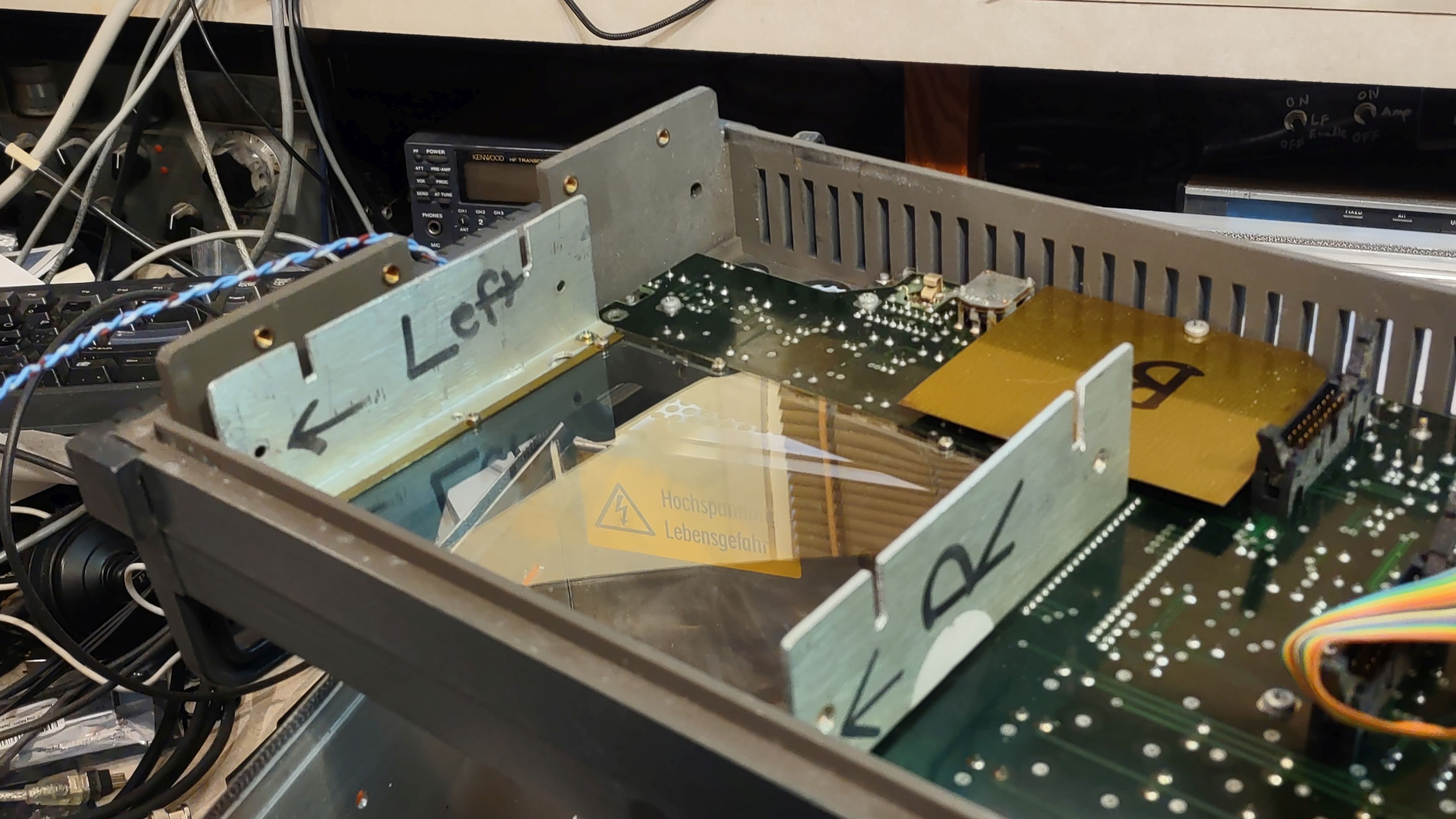
Mounting the boards:

Figure 20:
The "stack-up" of the boards on the mounting sled.  Hidden
by the ribbon cable is the sync processor, above that is the
the GBS-8300 with its output VGA connector and above
that is the LCD controller with 4-button daughter board.
At the bottom, on the sled, may be seen the 7812
regulator used to drop the 15 volt supply to 12 volts.
Click on the image for a larger version.
A "sled" about 6" (155mm) wide and about 4.75" (120mm) tall - designed to be mounted to the left-hand wall (as viewed from the front panel) inside the enclosure.  This was constructed from a sheet of scrap aluminum and on it, the sync processor board, the GBS-8200 and the LCD controller were mounted using an assortment of stand-offs.  The different shapes and sizes of these boards complicated matters, so I had to be creative, resorting to mounting the LCD controller - and its daughter board (with pushbuttons and infrared receiver) to a piece of glass-epoxy PCB material that was, itself, held in place with stand-offs, seen in Figure 20 as the board on the vary top.

While I happen to have a bunch of stand-offs in my parts bins, I could have just as easily mounted the boards using long screws or "allthread" along with an assortment of nuts and washers.  These days, a more elegant custom mount could also be 3D-printed to hold these boards in place, although the metal "sled" and stand-offs offer a solid electrical connection to the chassis that may aid in RFI shielding and mitigation.

The only critical things in mounting are to provide access to the ICSP connector and R1 ("gray" adjust) on the sync processor board, the buttons on the GBS-8200, and the buttons on the daughter board on the LCD controller:  All of these should be accessible with just the top cover of the 4031 removed, without needing to disassemble anything else as depicted in Figure 21.

Figure 21:
Installed and powered- up, the stack-up of boards and
connected LCD panel.  All controls - and the ICSP
connector - are accessible simply by removing the top cover
of the 4031.
Click on the image for a larger version.
Into this "sled" were pressed self-retaining "PEM" nuts and it is mounted at four points in the same slots (using 8-32 screws) on the left side of the frame that were used to mount the original CRT monitor.

Powering the boards:

As noted above, the GBS-8200 is available in a version that may operate from 5-12 volts.  Similarly, the LCD panel's board can also accommodate up to 12 volts - but the 4031 supplies 15 volts.  During development, I ran both boards on the 4031's 15 volt supply directly with no issues, but I noted that 16 volt electrolytic capacitors were used on the inputs, so 15 volts would be pushing their maximum ratings.

Despite having no issues, I decided not to take a chance, so I added a 7812 voltage regulator, bolting it to the aluminum "sled" for heat-sinking (see Figure 20) and powering both the GBS-8200 and LCD panel from it.  As seen from the diagram above, the sync processor includes its own regulator (a 7805) and it may be powered from either 12 or 15 volts.

Overall results

Figure 22:
Under the shield of the "Monitor Control" board is R16, the
"width" adjustment that may be use to optimize video quality.
Click on the image for a larger version.

The results of all of this work look quite good as can be seen in the picture gallery below, but there are slight visual artifacts owing to the fact that the VGA conversion is from a device (the '4031) that does not have its pixel clock synchronized with the sampling clock of the GBS-8200 - or even the horizontal sync pulse.  The inevitable result is - if you look closely - that you may see some slight "glitching" on the leading or falling edge of vertical lines.

This effect can be reduce somewhat by adjusting the read-out pixel clock from the 4031's Monitor Control board.  Located on this board, under the shield, is potentiometer R16.  Nominally set to 11.0 MHz (as monitored at test point "Mp10") the frequency of this clock output may be reduced by turning this potentiometer slightly clockwise, reducing the effects of this aliasing somewhat by increasing the "width" of the display by making it output the line of video "slower".

If this adjustment is done, it should be done iteratively:  If it is set too low, the beginning of the line will start before the current line has finished drawing causing you to be able to see the left edge of the screen along the far right edge.  By adjusting the "Horizontal Width" on the GBS-8200, some of this overlap can be moved off the right edge of the screen so a balance between this and a low clock frequency must be found.  The approximate frequency set by R16 after this adjustment is between 7.75 and 8.0 MHz.

As mentioned earlier, trying to set a color horizontally across a scan line is not really practical:  The fact that, as we have seen, the pixel read-out rate is a free-running oscillator that is not synchronous with any of the the video sync pulses, so there is no "easy" way to synchronize a clock signal to set color attributes along the scan line from the video information alone.  To do so would require a sample of the pixel clock itself from the Monitor Control board!

In theory, it may be possible to tie the internal pixel clock to an already-existing clock signal on the Monitor Control board (e.g. the 8 MHz clock) to allow this and to reduce the "glitching" that is sometimes visible:  This modification is open to investigation.


Photo gallery

The following are screen captures obtained by first connecting a VGA-to-HDMI converter to the VGA output of the GBS-8200 board, and then connecting the HDMI output to a USB3 HDMI capture device meaning that the image is re-sampled several times in the process, accumulating artifacts. 


Figure 23:
The main "RX FM" screen.  The top portion is colored as light magenta to indicate an RX-FM screen while the center portion is colored in yellow.  The "soft" buttons on the bottom of the screen are given the attribute of a "gray" color.
Click on the image for a larger version.


Figure 24:
The TX FM screen, the top portion color-coded as light-cyan.
Click on the image for a larger version.


Figure 25:
The "duplex" screen, the top portion color-coded as light-green.
Click on the image for a larger version.

Figure 26:
The "oscilloscope" screen.  Because it is an "RX FM" screen, the top portion is colored with light-magenta, with the portion with the scope trace is colored light yellow.
Click on the image for a larger version.

Figure 27:
The analyzer display, color coded as light cyan as it's one of the "TX FM" modes.
Click on the image for a larger version.

Figure 28:
The Modulation Monitor "Zoom" screen, color coded as light magenta as it's one of the "RX FM" modes.
Click on the image for a larger version.


Video captured from the 4031:

Here is a short video,captured from the output of the GBS-8200, as the various screens are selected on the 4031:


At the end of the video, the monochrome modes (green, yellow, etc.) are selected in sequence.

Remember:  The video on the LCD mounted in the 4031 looks quite a bit better than is represented in the video - not only because it's a smaller screen, but the capturing of the video from the VGA output added yet another stage of analog digitization/degradation - plus there are artifacts from the YouTube video compression as well.

* * * * * * * * * * * * * * * * 

Why use a PIC?

One might ask, "Why did you do this with a PIC rather than an Arduino or a Raspberry Pi?"

First, I've been using the PIC Microcontrollers since the early 1990s, making good use of the CCS "PICC" compiler - (LINK) for much of this time:  This compiler is capable of producing fairly tight and compact code and I'm very familiar with it.  The PIC16F88 was chosen because it has the necessary hardware peripherals, it's easy to use, has plenty of RAM, program space and speed for this task, and is still available in DIP (and SMD) packages - a real plus in these days of "supply chain" issues.

The code running on the PIC uses interrupts and as such, it's possible that its same function could be done on a lower-end Arduino UNO as that processor sports similar hardware capabilities - but it's unlikely that this could be done using the typical Arduino IDE sketch environment, which does not, by default, lend itself to latency-critical interrupt processing.  You would have to get much closer to the "bare metal" and implement lower-level interrupts and some careful coding (possibly in mixed "C" and assembly) in order to have the code operate fast and consistently enough to do the pixel counting.

Another possibility is to use an ESP8266 or ESP32, but again one would need to get closer to the "bare metal" and optimize timing of the code to handle this sort of task - and you would still need to have the same sort of hardware (sync reprocessor, control of the RGB) signals.

Finally, a Raspberry Pi - if you can get one - would be overkill - and it would take MUCH longer for the RPi to boot up than the service monitor, which is up and running in under 15 seconds from power-up:  You would still need to interface the same signals (sync, video), but to 3.3 volt logic, and you would still need the same hardware (analog switches, etc.) to modify the video attributes - not to mention the time-critical code on a non-realtime operating system to do the pixel counting but this task could be done with additional hardware if needed.

Where can I get the code?

You may find the source code (for the CCS "PICC" compiler - I used version 5.018) and a compiled .HEX file for the PIC16F88 at the following links:

The .HEX code above is suitable for "burning" into a PIC16F88, and I use the PicKit3 programmer's ICSP (In Circuit Serial Programming) for this:  It's possible to reprogram the device in a powered-up 4031 - but because the code is written to detect when the ICSP is connected, it won't resume normal operation until the cable is disconnected.

As mentioned before, I have only one version of the 4031, so if your device has "different" screen signatures that result in pixel counts that don't match what's in the code, that screen will be rendered with white text.  Due to the complexity of the screen detection via pixel counting, making the recognition of the screen an automated process so that one could provide user-defined configurations would require a significant addition to the code - and likely the need for much more code space.

With the information provided it should be possible to apply this technique using other hardware platforms/microcontrollers - provided that one has either the speed to reliably count pixels at MHz rates and/or is able to get close enough to the "bare metal" of the processor to use on-chip peripherals to aid in the task.  In either case, close attention to the way the code operates - possibly a bit of optimization - will likely be required to pull off this task.

Final comments:

The most obvious change in the appearance of the 4031 after the modification - other than the colorized screen - is that of readability.  Clearly, the replacement of the degraded screen protector improved things considerably!

One advantage of the CRT - assuming that it is in good condition - is that it can be very bright, meaning that the LCD is at a slight disadvantage where high ambient light might be an issue:  In this case, one of the available "monochrome" modes may help.

The most obvious disadvantage of the LCD is that unlike the CRT, which has essentially a Lambertian emission profile from its surface (e.g. it radiates light hemispherically from the plane of the surface of the CRT), the LCD, by its very nature, has a comparatively reduced viewing angle.

When faced with viewing difficulties one would, in practice, simply relocate or reposition the 4031 so that it was more favorably oriented - and in some instances switching to one of the large "Zoom" screens may help when reading from a distance and/or awkward angle:  If you wish to do so, you could take advantage of the ability to use an external LCD monitor (small 7" units are fairly inexpensive) as described above.

Installing an LCD panel - with a blemish-free screen protector - and having "colorized" screens is a nice "refresh" of the 4031, particularly if you have been dealing with an ailing CRT for which there is no modern, drop-in equivalent.

* * * * * * * * * * *

This page stolen from ka7oei.blogspot.com


[END]


Improving my ultrasonic sniffer for finding power line arcing by using MEMs microphones

By: Unknown
1 August 2022 at 04:18

Figure 1:
The packaged MEMs microphone, along with the
ultrasonic receiver.
Click on the image for a larger version.

Years ago - probably 20+ - I constructed a superheterodyne "Bat Listener" to eavesdrop on the goings-on of our winged Chiroptera friends.  (That receiver - the one depicted in Figure 1 - is described HERE.

In retrospect, this device is probably a lot more complicated than it need be as it up-converts from "audio" to a 125 kHz IF, using a modified 262.5 kHz Philco (Ford) car radio IF Can as the filtering element before being converted back down to audio.  This device has a built-in microphone, but it also has a jack for an external microphone, which comes in useful.

This device actually works pretty well for its intended purpose and, in a pinch, can even be used to listen to LF and VLF signals like the time station WWVB at 60 kHz and the powerful transmissions intended for submarines in the 20-40 kHz range if a simple wire is attached to the external microphone input, but I digress.

One of the weak points of this unit has always been the microphone.  To be sure, there exist the 40 kHz ultrasonic transducer modules:  These units used to be common in TV remote controls before the Infrared versions became common and you might still find them in the (now rare-ish) ultrasonic intrusion alarms.  While fairly sensitive, these units do have a "problem":  They are rather sharply resonant around their design frequency - which is typically somewhere around 40 kHz.  In other words, they aren't very good over much of the ultrasonic frequency range above or below 40 kHz.

It would seem that many commercial ultrasonic power mains arc detectors use these things (The MFJ-5008 seems to be an example of one of these) and there have been a few articles on how to make these devices (See the April, 2006 QST article, A Home-made Ultrasonic Power Line Arc Detector - link) but it, too, uses one of these "narrowband" 40 kHz transducers.

While certainly fit for purpose, I was more interested in something that could be used across the ultrasonic spectrum.  When I built my "bat listener" I fitted it with a "condensor" (electret) microphone, rummaging through and trying each of the units that I'd accumulated in my parts box at the time to find the one (make and model unknown) that seemed to be the most sensitive - but compared to a 40 kHz transducer, it was still somewhat "deaf".

This issue has nagged at me for years:  I occasionally break out the "bat listener" to (would you believe) listen for bats and other insects when camping, and it is useful if you have a suspected air leak in a compressed air system - plus it's sometimes just plain interesting to walk around the house and yard to hear what's happening at frequencies beyond human hearing - and it may also be used for finding arcing power lines as the QST article referenced above suggests.

In more recent years, an alternative to the electret microphone has appeared on the scene in the form of the MEMS (MicroElectricroMechanical System) microphone.  This class of devices are literally tiny mechanical devices embodied in silicon structures and they can range from oscillators to accelerometers to exotic tiny motors to (you guessed it) - microphones.  Their small size, which makes them the choice when space is at a premium, as in the case of a phone or web camera, also reduces the mass of the the mechanical portion that responds to variations in air pressure (e.g. sound) which can enable them to respond to frequencies from a few 10s of Hertz to well into the 10s of kHz.

Figure 2:
The MEMs microphone mounted and wired up.  The element
is mounted "dead bug" by gluing its top side to the circuit
board and small (#30) wires connect to the pads.
Click on the image for a larger version.

Perusing the data sheets of devices found on the Mouser Electronics web site, I found what seemed to be (one of many) suitable candidates:  The Knowles SPU0410LR5H-QB.  This device, which is a version with an analog output, is about 3mm by 4mm, has a rated frequency response to at least 80 kHz - and it is pretty cheap:  US$ 0.79 each in single quantities at the time of this writing - and, in these days of erratic supply lines, it was available immediately as Mouser reported having more then 30k of them in stock.  

Importantly, this device had its "audio port" on the same side as the wiring - the intention being that it would get its sound through a hole in the circuit board, but this would also make it easier to wire up as described below.

The fact that this is a small, surface-mounted device may seem daunting to the home building - but don't be daunted:  Given the appropriate magnification device (I use a pair of "Geezer Goggles" that I got from Harbor Freight) and a fine-tipped soldering iron, it's perfectly reasonable to solder just a few fine (30 gauge) wires to a device this small.

Figure 3:
The completed board, containing the circuit depicted in
Figure 4, below.  The board with the microphone is on
the left, and the attaching cable is seen in the upper-right.
LED1, the one across the microphone element itself,
was mounted on the bottom side of the board.
Click on the image for a larger version.

First, I cut a small piece of circuit board material to use as a substrate and mounted at a right angle on a larger piece, as shown.  I then took the microphone and "Super Glued" it "dead bug" to the middle of this board (see Figure 2, above) leaving the side with the connections and sound port facing outwards.

With this simple operation, a very tiny part suddenly becomes a larger, easier-to-manage part - albeit with very closely-spaced wire connections.  Being careful with very thin solder not to get any solder or flux in the sound port, I first tinned the connections on the device itself (there are four pads - two grounds, a power and an audio) and then proceeded to use some #30 "wire wrap" wire to make flying lead connections to the device, using a slightly longer section of one to tie the two "grounds" together.  I could have just as easily used some tinned #30 enameled wire, instead, but I tend to keep the Kynar-covered wire wrap wire on-hand for this very purpose.  

With the flying leads and the piece of circuit board as a "breakout" device, I was then free to treat the MEMs microphone as a "normal sized" device and build an interface circuit onto the rest of the board.

In perusing the data sheet, I noted that the power supply voltage rating was 1.5-3.6 volts which was incompatible with the 5 volts of "phantom power" applied by my bat listener to the microphone jack to power a condensor (electret) microphone, but this was easily remedied using the circuit shown below:

Figure 4:
The interface circuit used to adapt the MEMs microphone to the existing 5-volt
electrect microphone circuit.
Click on the image for a larger version.

Circuit description:

This circuit depends on there being power applied via the audio/microphone lead, as is commonly done for computer microphones.  Typically, this is done by biasing the audio line through a resistor (2.2-10k is common) from a 5 volt supply - and that is assumed to have been done here on the device to which this will be connected, as I did on my "bat listener".

DC is decoupled from the audio output of the microphone via C1.  In this circuit, I chose a 0.01uF capacitor as I wanted to reject audible frequencies (<10 kHz) to a reasonable extent - and this means that this capacitor value is way too small if you plan to use it as a "normal" microphone to listen well down into the lower audible range:  Something on the order of 1-10 uF would be appropriate if you do want audio response down to a few 10s or 100s of Hz.

A word of warning:  Do NOT use a ceramic capacitor for C1 as these can be microphonic in their own right.  I used a 0.01uF plastic capacitor (probably polyester) which is neither microphonic or prone to change capacitance wildly with temperature.

Resistor R1 (2.2k shown here, but anything from 2.2k to 4.7k would likely be just fine) decouples the audio from the DC and capacitor C2 removes that audio, providing a "clean" power source for the microphone.

Here, LED2 is used as a voltage limiter:  Being an "old fashioned" green panel indicator LED, its forward voltage is somewhere around 2 volts.  The use of an LED in this manner has the advantage that unlike a Zener, this type type of LED has a very sharp "knee" and practically no leakage current below its forward voltage - and it is much easier to find than a 2-2.5 volt Zener.  It's likely that about any LED would work here - including a more modern Gallium Nitride type (e.g. blue, white, super bright green) but I have not verified that they would properly clamp the voltage in the 1.5-3.6 volt range needed by the microphone.  (And no, there are not any detectable effects on the circuit from light impinging on the LEDs.)

LED1 is present to protect the microphone itself.  When it's plugged in, whatever voltage is present on the audio cable will be dumped into the microphone output as capacitor C1 is charged and it could damage it, particularly if the power source is 5 volts and the microphone's maximum rated voltage is just 3.6 volts.  This LED, which is the same type as LED2, will not normally conduct as the audio output from the microphone typically has a voltage of roughly half that of the supply, so LED1 will be completely "invisible" (in the electrical sense) in normal operation.

Figure 5:
A spring, soldered to a wire connecting to the "ground"
side of the circuit (also the microphone cable shield)
used to make contact with the aluminum tubing.
Click on the image for a larger version.

I mounted the board with the microphone in a piece of aluminum tubing that would fit the microphone mount of my parabolic dish (see below) and this not only provides protection for the microphone and circuitry, but also serves as an electrostatic shield, preventing energy - say, from a power line - getting into the circuitry.  To make this effective, the tubing itself is connected to the ground lead (cable shield) by soldering a wire to a metal spring and placing it in the end of the tubing as seen in Figure 5.

To secure things into place, a bit of "hot melt" glue was used, preventing the board from sliding out.  The connection to the receiver was made via a length of PTFE (Teflon) RG-316 coaxial cable - but shielded audio cable would have sufficed:  This cable is firmly attached to the board as seen in Figure 3 as a strain relief. 

The parabola:

While the microphone is sensitive in its own right, its sensitivity can be noiselessly "amplified" many-fold by placing it at the focus of a parabolic dish.  I was fortunate to have obtained a Dan Gibson EPM model P-200 (minus the original microphone element or any electronics, but including the holder) at a swap meet, but the QST article linked above suggests other sources - and I have seen parabolic-based microphones on Amazon - often as semi-serious toys - as well.  Using the holder - the inner diameter of which was the basis for choosing the specific size of the aluminum tubing - the microphone was mounted at the focus of the dish.

Finding this focus can be a bit of a challenge without the proper equipment, so I set up a "test range".  At one end of my back yard I placed a 40 kHz transducer (of the sort noted in the QST article linked above) connected to a function generator set to 40 kHz:  I'm sure that a small speaker would have been sufficient to generate a signal.

Figure 6:
The MEMs microphone, mounted in the aluminum
tubing, at the focus of the parabolic dish, with attached
cable.
Click on the image for a larger version.

From across the yard - perhaps 30 feet (10 meters) away, I sighted the emitter through the dish, using its alignment dots and slid the microphone in and out until I had the best combination of the loudest signal, the sharpest aiming, and the "cleanest" pattern.  On this last point, I noted that if I focused too far in our out, the peak of the signal would become "blurry" (e.g. spread out) or, in some cases, I would get two peaks - one on either side of the "real" one, so the object was to have the single, loudest peak possible.  Once this was found, it was marked and a bit of heat-shrink tubing was put over the end of the aluminum tube, corresponding with that mark, to act as a "stop" to set the correct focus depth.

Again, refer to the QST article linked above for additional advice on where to obtain a suitable parabolic reflector, and hints on the mechanical construction.

Does it work?

The answer is yes.  From significant distances, I can hear the acoustic signature of switching power supplies (apparently, many of these have transformers that vibrate at their 30-60 kHz switching frequency) as well as the sounds of insects, and the hissing of the capillary valve of the neighbor's window air conditioner.

Importantly, I was able to verify that a power pole's hardware was, in fact, arcing slightly - although I wasn't able to determine which hardware, exactly was making the racket as it was quiet enough that it became inaudible when I stood far enough away from the (tall!) pole to get a better viewing angle.

When I get the chance, I will replace the capsule electret microphone built into the receiver itself with one of these MEMs units, but that's just one project on a rather long list!

This page stolen from ka7oei.blogspot.com

[End]


The use case for a blinking infrared LED

By: Unknown
29 June 2022 at 14:27

Many years ago at a company where I worked, we had two sets of computer systems:  The ones that we used every day for engineering purposes, and the "corporate" computers that were used for things like "official" email and interfacing with accounting.

Figure 1:
The IR (clear) LED and the red blinking LED.
The red LED was uncovered for this picture.  The IR
LED is positioned to stick up, inside the mouse's lens
assembly when it's placed atop the pad.
Click on the image for a larger version.
One day, the edict came from on-high that the corporate computers would log themselves off the network after a ridiculously short amount of time (it may have been as little as 5 minutes) if no mouse or keyboard activity was used.

This was particularly bothersome to the local accountant person who would have to turn away from the corporate computer for a few minutes at a time to do something else (paperwork, answer a phone, etc.) only to find that it had logged off and out of whatever application was running.  To make matters worse, it took several minutes to log back in as the authentication was painfully slow:  This was way back in the late 1990s/early 2000s, you know!

Comment:

It should go without saying that absurd and draconian "security" measures like those described above are usually self-defeating:  It adds unnecessary frustration to those using the system, causing "creative" means to be derived to circumvent it which can completely defeat the intent of the measures.  It had already been the practice of the person using this computer to log off when stepping out of the office (and locking the door!) but we heard of other "interesting" ways that others came up with to circumvent this within the company. 
Fortunately, it was only a few months later that the computer security folks came up with a much more sensible plan and the device described here was no longer "needed".
After several weeks of being frustrated by this - and being denied the request to lengthen the auto-logoff to something more reasonable like 10-30 minutes, I was asked if there was something that I could do.  The first thing that I thought of was some motorized do-hickey that would move the mouse just a little bit to make it "look" like the computer was in use - but something else occurred to me:  Interfere with the optical mouse in some way externally.  This method had the advantage that no device was plugged into the computer (e.g. an external "mouse jiggler" USB device) - an advantage in that there is no possibility of such a device, itself, causing a security risk.

Modern optical mouses (mice?) literally take a picture of the desktop - many times a second - and divine the movement by tracking very small features under them.  Fortunately most surfaces have small-scale features that make this possible - but if you were ever wondering why an optical mouse doesn't work well on a piece of clean glass - now you know!

Figure 2:
The optical mouse atop the IR LED.  The IR LED fits
up inside the lens cavity.  The entire circuit was inserted
and built into a piece of scrap mouse pad.
Click on the image for a larger version.
So, how would one make the think the mouse is moving - without actually moving it?  It occurred to me that a flashing, red LED would accomplish this by, perhaps, "blinding" the sensor - at least partially.  A quick test by sticking the blinking LED up into the lens assembly showed that as it blinked, the cursor would move one "Mickey" (the unit of mouse movement - look it up!) up and to the right on this particular mouse, satisfying the computer that the mouse was actually being moved.  It didn't seem to matter that the mouse cursor would inevitably end up in the top-right corner of the screen - it seemed to stop the time-out nonetheless.

This worked well - but what if a blinking LED bothers you?  The answer is a blinking infrared LED.

Where does one get a blinking Infrared LED?

Of course, no-one makes such a thing (why would they?) - but the work-around is simple:  Place an ordinary infrared LED in series with a visible blinking one and place the latter LED out of sight.

Infrared LEDs - which may be harvested from defunct/surplus infrared remotes - come in two flavors:  Those that operate at 850 nanometers, and those that operate at 940 nanometers.  The 850 nanometer versions are just visible to the human eye (in a dark room) and work best in this situation as they are well within the response curve of the sensor in the mouse but can't really be seen in normal room lighting:  In fact, some optical mouses (mice?) use Infrared LEDs to be more "stealthy".  I didn't try a 940 nanometer LED, but I know from experience that if something operates on a visible (red) wavelength, it will likely work just fine with an 850 nanometer LED.

The circuit to do this was very simple, and is as follows:

Figure 3:
Diagram of the circuit - pretty simple, actually!
As noted, the voltage can be anywhere between 9 and 15 volts DC - 12 volts nominal.
Click on the image for a larger version.

The power supply used was a random "wall wart":  The one that I'd grabbed was marked 9 volts at 100 milliamps and it put out about 13 volts DC under no load, but any DC voltage between 9 and 15 volts ought to be fine:  5 volts from a USB charger is simply too low!

The way this works is that with the two LEDs in series, the current in the two LEDs MUST be identical (Kirkhoff's law and all of that...) which means that when the blinking LED was on, more current also went through the other LED, making it brighter.  When the blinking LED was off, the other LED doesn't go completely off, but it gets noticeably dimmer - which was enough to make the mouse detect "movement".  The 470 ohm resistor limits the current to a safe value and the 100 uF capacitor provides a bit of bypassing that helps assure that the blinking LED will function properly:  It may work without it - but not all blinking LEDs do.  Because they are in series, it doesn't matter the order in which the LEDs are placed - just that they are in series and connected correctly in terms of polarity.

If you are unsure that the infrared LED is blinking, check it with your cell-phone camera as it will respond adequately to Infrared, particularly up-close, and with 850 nanometer LEDs.

This trick also works with other LEDs:  If you have a cheap, red blinking LED but not one of the color that you might want to blink (say a white or blue LED) this could be substituted for the "IR LED".  Again, the "other" (non-blinking) LED may not extinguish completely during the "off"portion and if this bothers you, a resistor could be placed across it to "bridge" some of the current around it (e.g. the non-blinking LED) and drop the voltage below its illumination threshold:  The value would have to be experimentally determined.

There you go:  A use-case for a blinking infrared LED!

* * *

This page stolen from ka7oei.blogspot.com


[END]


Fixing a TS-570G (The tuner couldn't find a match, timing out...)

By: Unknown
29 May 2022 at 02:25

The TS-570D's front panel

 A couple of months ago I happened to be at a swap meet in Northern Utah and talking to a gentlemen - with whom I had a passing acquaintance - as he was unloading his vehicles.  One of the things that he placed on his table was a Kenwood TS-570D, in its original box, with a price tag on it that seemed to be too good to be true.

Asking about it, he said that it worked fine, but that the "tuner wouldn't stop", so it had to be used with the antenna tuner bypassed.  Visually inspecting it, it looked to be in "good nick" (a 4 out of 5) so I shut up and gave him the money.

After digging out from underneath a few other projects, I finally took a look at it and sure enough, pressing the AT TUNE button started a bout of furious clicking that didn't stop for about 30 seconds with the radio beeping an error.  I couldn't help but notice, however, that there was no SWR or power output indication while the tuner was doing its thing - but if I bypassed the tuner, both of these were true.

Going into the menu (#11 - "Antenna tuner operation while receiving") I set that to "on" and noticed that the receiver went mostly dead - a sure sign that something was amiss with the signal path through the tuner.  Popping the covers, I whacked on the relays with the handle of a screwdriver while the radio was connected to an antenna and could hear signals come and go.  This attempt at "percussive repair" quickly narrowed the culprit to relay K1, the relay that switches the antenna tuner in and out of the signal path.

A few weeks later, after having ordered and receive a new relay, I cleared enough space on the workbench to accommodate the radio and commenced a repair.

The repair:

The antenna tuner is on the same, large circuit board as the final and low-pass filter, which meant that not only were there a zillion screws to take out, but I also had to remove the white thermal heat-sink compound from several devices, un-clip the back panel connectors and un-plug a few signal cables.  Using my trusty Hakko DFR-300 desoldering gun, I was able to cleanly remove both K1 and - because I had two relays, and they were identical - K3 as well, soldering in the replacement.

When I'd pulled the board, I also noticed that components "D10" - which is a glass discharge tube across Antenna connector #2 - had some internal discoloration, possibly indicating that it had seen some sort of stress, so I rummaged about and found two 350 volt Bourns gas discharge tubes and replaced both "D10" and "D11" - the unit on the Antenna #1 connector.  Unlike the originals - which are glass - these are metal and ceramic, requiring that I put a piece of polyamide (a.k.a. Kapton) tape on the board to insulate them from the traces underneath.  The leads of these new devices were also much heavier and would not fit through the board (drilling larger would remove through-plating!) so I soldered short lengths of #24 tinned wire through the holes and used these to attach the straight leads of the new discharge tubes.

After cleaning the board of flux with denatured alcohol and an old toothbrush, I put an appropriately sparse amount of heat sink compound on the required devices, loosely started all of the screws and with everything fitting, I snugged them all down, finishing with the RF output transistors - and then re-checking everything again to make sure that I didn't miss anything.

After plugging the connecting cables back in I noted that the receiver now worked through the tuner and pressed the AT Tune button and was greeted with lots of clicking and varying VSWR - but still, it continued and eventually errored out.

Figuring that the radio's computer may have been messed up, I did a complete CPU reset, but to no avail.  Because the SWR and power indication were working correctly, I knew that this wasn't likely to be a component failure like the reverse power detection circuit, so it had to be something amiss with the configuration, so I referred to the service manual's section about the "Service Adjustment Mode".

Going through the Service Adjustment Mode Menu:

Like most modern radios, this one has a "Service Menu" where electronic calibration and adjustments are performed and to get to it, I inserted a wire between pins 8 and 9 of the ACC2 jack and powered up the radio while holding the N.R. and LSB USB keys and having done this, a new menu appeared.  On a hunch, I quickly moved to menu #18 - the adjustment for the 100 watt power level.

What is supposed to happen is that if you key the radio, it will transmit a 100 watt carrier on 14.2 MHz, but instead, I got about 60 watts, and checking the related settings for 50, 25, 10 and 5 watts, I got very low power levels for each of those as well.  To rule out an amplifier failure, I went back to the 100 watt set-up and pressed the DOWN button, eventually getting over 135 watts of output power, indicating that there was nothing wrong with the finals, but rather that the entire "soft calibration" procedure would have to be followed.

Starting at the beginning of the procedure which begins with receiver calibration, I found everything to be "wrong" in the software calibration, indicating that either it was improperly done, or the original calibration had somehow been lost and replaced with default values.  I checked a few of the hardware adjustments, but found them to be spot on - the exception being the main reference oscillator, which was about 20 Hz off at 10 MHz, which I dialed back in, chalking this up with aging of the crystal.

During the procedure, I was reminded by a few peculiarities - and noticed some likely errors, and here they are in no particular order:

  • Many of these menu items are partially self-calibration, which is to say that you establish the condition called out in the procedure and push the UP or DOWN button.  For example, on menu item #16 where the Squelch knob is calibrated, one merely sets it to the center of rotation, the voltage is shown on the screen in hexidecimal, and you press the button and the displayed value is stored temporarily in memory.
  • I'm a bit OCD when it comes to S-meter calibration, preferring my S-units to be 6 dB apart, S-9 to be represented by a -73dBm signal as noted by the IRU specifications, and for "20 over" to actually be "20 over S-9", or around -53 dBm.  The procedure in the manual - and the radio itself doesn't permit this, exactly.
    • To set the "S1" signal level (menu item #3) would require a signal level -121 dBm, but the receiver's AGC doesn't track a signal below around -113 dBm.  Instead, I noted the no-signal level on the display when menu #3 was selected and then set the signal level to an amplitude that just caused the hexidecimal number to increase and then pushed the button, setting "S1" to be equivalent to the lowest-possible signal level to which the AGC reacts.
    • To set the "S9" signal level (menu item #4) I set the signal generator to -73dBm and pressed the button.
    • To set the "Full scale" level (menu item #5) I set the signal generator to -23 dBm and pressed the button.  If you have followed the math, you'll note that "Full Scale" - which is represented as "60 over" should really be -13 dBm, but I observed that the AGC seemed to compress a bit at this signal level and the "20 over" and "40 over" readings came out wrong:  Using a level of -23 dBm got the desired results.
    • NOTE:  The service menu forces the pre-amp to be enabled when doing the S-meter calibration (e.g. you can't disable it when in the service menu) so the S-meter calibration only holds when the pre-amp is turned on.
  •  For setting menu item #1, "ALC Voltage" I was stumped for a bit.  It mentions measuring "TP1" - but this is not the "TP1" on the transmitter board, but rather the TX/RX unit (the board underneath the radio).
  • I noticed that if step #7 was followed to set the 100 watt power level, it was difficult to properly set menu items 23-28 (the "TGC" parameters).  These adjustments set to 100 watts, but if you have already set menu item #18 at 100 watts, you can't be sure that you've properly done it.
    • The work-around is that prior to step #6 in the procedure that you go to menu item #18 and adjust for higher than 100 watts - say, 125 watts.  If this is done, you can adjust menu items 23-28 (noting that menu #27 is adjusted out-of-order in procedure step #6) to 100 watts.
    • Once procedure steps 6, 7 and 8 are done (but skipping the adjustment for menu #18 in step 7) you can go back to menu #18 and adjust for 100 watts.
  • For procedure steps 16 and 17, I didn't have a 150 ohm dummy load, but I did have several 50 ohm loads, so I put three of them in parallel - which yields 16.67 ohms, which is also a 3:1 VSWR - and completed these steps.  It's worth noting that Yaesu uses 16.67 ohms for the equivalent step in its alignment procedures.  To set the "40 watts" called out in step 17 I used the front-panel power meter, which would have already been calibrated in the procedure.

The result:

As mentioned, the "hardware" calibration seemed to be fine and only the "soft" calibration was off and after following this procedure, the tuner worked exactly as it should.  What I suspect was occurring was a combination of the the output power being too low to calculate an SWR (e.g. setting the radio to "5 watts" yielded less then 2) and that the SWR meter calibration itself was incorrect and that this combination of factors prevented the tuner from being able to find a match.

Since the repair, the TS-570 has been used several times per week and it is working just as it should!

This post stolen from ka7oei.blogspot.com

[End]


Implementing the (functional equivalent of a) Hilbert Transform with minimal overhead

By: Unknown
1 May 2022 at 05:07

I recently had a need to take existing audio and derive a quadrature pair of audio channels from this single source (e.g. the two channels being 90 degrees from each other) in order to do some in-band frequency conversion (frequency shifting).  The "normal" way to do this is to apply a Hilbert transformation using an FIR algorithm - but I needed to keep resources to an absolute minimum, so throwing a 50-80 tap FIR at it wasn't going to be my first choice.  

Another way to do this is to apply cascaded "Allpass" filters.  In the analog domain, such filters are used not to provide any sort of band-filtering effect, but to cause a phase change without affecting the amplitude and by carefully selecting several different filters and cascading them.  This is often done in "Phasing" type radios and this is accomplished with 3 or 4 op amp sections (often Biquad) cascaded - with another, similar branch of op-amps providing the other channel.  By careful selection of values, a reasonable 90 degree phase shift between the two audio channels can be obtained over the typical 300-3000 Hz "communications" bandwidth such that 40+ dB of opposite sideband attenuation is obtainable.

Comment: 

One tool that allows this to be done in hardware using op amps is Tonne Software's  "QuadNet" program which is an interactive tool that allows the input and analysis of parameters to derive component values - see http://tonnesoftware.com/quad.html .

I wished to do this in software, so a bit of searching let me to an older blog entry by Olli Niemitalo of Finland, found here:  http://yehar.com/blog/?p=368  which, in turn, references several other sources, including:

This very same same technique is also used in the "csound" library (found here) - a collection of tools that allow manipulation of sound in various ways.

My intent was this to be done in Javascript where I was processing audio real-time (hence the need for it to be lightweight) and this fit the bill.  Olli's blog entry provided suitable information to get this "Hilbert" transformation working.   Note the quotes around "Hilbert" indicating that it performs the function - but not via the method - of a "real" Hilbert transform in the sense that it provides a quadrature signal.

The beauty of this code is that only a single multiplication is required for each channel's filter - a total of eight multiplications in all for each iteration of the two channels - each with four sections - something that is highly beneficial when it comes to keeping CPU and memory utilization down!

As noted above, this code was implemented in Javascript and the working version is represented below:  It would be trivial to convert this to another language - particularly C:

* * *

Here comes the code!

First, here are the coefficients used in the allpass filters themselves - the "I" and the "Q" channels being named arbitrarily:

// Biquad coefficients for "Hilbert - "I" channel
  var ci1=0.47940086558884;  //0.6923878^2
  var ci2=0.87621849353931; //0.9360654322959^2
  var ci3=0.97659758950819; //0.9882295226860^2
  var ci4=0.99749925593555; //0.9987488452737^2
  //
  // Biquad coefficients for "Hilbert" - "Q" channel
  var cq1=0.16175849836770; //0.4021921162426^2
  var cq2=0.73302893234149; //0.8561710882420^2
  var cq3=0.94534970032911;  //0.9722909545651^2
  var cq4=0.99059915668453;  //0.9952884791278^2

Olli's page gives the un-squared values as it is a demonstration of derivation - a fact implied by the comments in the code snippet above.

In order to achieve the desired accuracy over the half-band (e.g. half of the sampling rate) a total of FOUR all-pass sections are required, so several arrays are needed to hold the working values as defined here:

  var tiq1=[0,0,0];  // array for input for Q channel, filter 1
  var toq1=[0,0,0];  // array for output for Q channel, filter 1
  var tii1=[0,0,0];  // array for input for I channel, filter 1
  var toi1=[0,0,0];  // array for output for I channel, filter 1
  //
  var tiq2=[0,0,0];  // array for input for Q channel, filter 2
  var toq2=[0,0,0];  // array for output for Q channel, filter 2
  var tii2=[0,0,0];  // array for input for I channel, filter 2
  var toi2=[0,0,0];  // array for output for I channel, filter 2
  //
  var tiq3=[0,0,0];  // array for input for Q channel, filter 3
  var toq3=[0,0,0];  // array for output for Q channel, filter 3
  var tii3=[0,0,0];  // array for input for I channel, filter 3
  var toi3=[0,0,0];  // array for output for I channel, filter 3
  //
  var tiq4=[0,0,0];  // array for input for Q channel, filter 4
  var toq4=[0,0,0];  // array for output for Q channel, filter 4
  var tii4=[0,0,0];  // array for input for I channel, filter 4
  var toi4=[0,0,0];  // array for output for I channel, filter 4


The general form of the filter as described in Olli's page is as follows:

 out(t) = coeff*(in(t) + out(t-2)) - in(t-2)

In this case,  our single multiplication is with our coefficient being multiplied by the input sample, and from that we add our output from two operations previous and subtract from that our input value - also  from two operations previous.

The variables "tiq" and "toq" and "tii" and "toi" refer to input and output values of the Q and I channels, respectively.  As you might guess, these arrays must be static as they must contain the results of the previous iteration.

The algorithm itself is as follows - a few notes embedded on each section


  tp0++;        // array counters
  if(tp0>2) tp0=0;
  tp2=(tp0+1)%3;

// The code above uses the modulus function to make sure that the working variable arrays are accessed in the correct order.  There are any number of ways that this could be done, so knock yourself out!

// The audio sample to be "quadrature-ized" is found in the variable "audio" - which should be a floating point number in the implementation below.  Perhaps unnecessarily, the output values of each stage are passed in variable "di" and "dq" - but this was convenient for initial testing.

  // Biquad section 1
  tii1[tp0]=audio;
  di=ci1*(tii1[tp0] + toi1[tp2]) - tii1[tp2];
  toi1[tp0]=di;

  tiq1[tp0]=audio;
  dq=cq1*(tiq1[tp0] + toq1[tp2]) - tiq1[tp2];
  toq1[tp0]=dq;

  // Biquad section 2
  tii2[tp0]=di;
  tiq2[tp0]=dq;
 

  di=ci2*(tii2[tp0] + toi2[tp2]) - tii2[tp2];
  toi2[tp0]=di;
 

  dq=cq2*(tiq2[tp0] + toq2[tp2]) - tiq2[tp2];
  toq2[tp0]=dq;

  // Biquad section 3
  tii3[tp0]=di;
  tiq3[tp0]=dq;
 

  di=ci3*(tii3[tp0] + toi3[tp2]) - tii3[tp2];
  toi3[tp0]=di;
 

  dq=cq3*(tiq3[tp0] + toq3[tp2]) - tiq3[tp2];
  toq3[tp0]=dq;

  // Biquad section 4
  tii4[tp0]=di;
  tiq4[tp0]=dq;
 

  di=ci4*(tii4[tp0] + toi4[tp2]) - tii4[tp2];
  toi4[tp0]=di;
 

  dq=cq4*(tiq4[tp0] + toq4[tp2]) - tiq4[tp2];
  toq4[tp0]=dq;

// Here, at the end, our quadrature values may be found in "di" and "dq"

* * *

Doing a frequency conversion:

The entire point of this exercise was to produce quadrature audio so that it could be linearly shifted up or down while suppressing the unwanted image - this being done using the "Phasing method" - also called the "Hartley Modulator" in which the quadrature audio is mixed with a quadrature local oscillator and through addition or subtraction, a single sideband of the resulting mix may be preserved.

An example of how this may be done is as follows:

  i_out = i_in * sine + q_in * cosine;
  q_out = q_in * sine - i_in * cosine;

In the above, we have "i_in" and "q_in" - which are the I and Q audio inputs, which could be our "di" and "dq" samples from our "Hilbert" transformation and with this is an oscillator with both sine and cosine outputs (e.g. 90 degrees apart).

These sine and cosine value would be typically produced using an NCO - a numerically-controlled oscillator - running at the sample rate of the audio system.  In this case, I used a 1k (1024) entry sine wave table with the cosine being generated by adding 256 (exactly 1/4th of the table size) to its index pointer with the appropriate modulus applied to cause the cosine pointer to "wrap around" back to the beginning of the table as needed.

If I needed just one audio output from my frequency shifting efforts, I could use either "i_out" or "q_out" so one need not do both of the operations, above - but if one wanted to preserve the quadrature audio after the frequency shift, the code snippet shows how it could be done.

* * *

Does it work?

Olli's blog indicates that the "opposite sideband" attenuation - when used with a mixer - should be on the order of -43 dB at worst - and actual testing indicated this to be so from nearly DC.  This value isn't particularly high when it comes to the "standard" for communications/amateur receivers where the goal is typically greater than 50 or 55 dB, but in casual listening, the leakage is inaudible.

One consequence of the attenuation being "only" 43 dB or so is that if one does frequency shifting, a bit of the local oscillator used to accomplish this can bleed through - and even at -43 dB, a single, pure sine wave can often be detected by the human ear amongst the noise and audio content - particularly if there is a period of silence.  Because this tone is precisely known, can be easily removed with the application of a moderately sharp notch filter tuned to the local oscillator frequency.

This page stolen from ka7oei.blogspot.com

[End]


High power Tayloe (a.k.a. Wheatstone) absorptive bridge for VSWR indication and rig protection.

By: Unknown
28 February 2022 at 05:35

Figure 1:  The completed absorptive VSWR bridge.
Last year, I was "car camping" with a bunch of friends - all of which happened to be amateur radio operators.  Being in the middle of nowhere where mobile phone coverage was not even available, we couldn't resist putting together a "portable" 100 watt HF station.  While the usual antenna tuner+VSWR meter would work fine, I decided to build a different piece of equipment that would facilitate matching the antenna and protecting the radio - but more on this in a moment.

A bit about the Wheatstone bridge:

The Wheatsone bridge is one of the oldest-known types of electrical circuits, first having been originated around 1833 - but popularized about a decade later by Mr. Wheatstone itself.  Used for detecting electrical balance between the halves of the circuit, it is useful for indirectly measuring all three components represented by Ohm's law - resistance, current and voltage.

Figure 2:  Wheatstone bridge (Wikipedia)
It makes sense, then, that an adaptation of this circuit - its use popularized by Dan Tayloe (N7VE) - can be used for detecting when an antenna is matched to its load.  To be fair, this circuit has been used many decades for RF measurement in instrumentation - and variations of it are represented in telephony - but  some of its properties that are not directly related to its use for measurement that make it doubly useful - more on that shortly.

Figure 2 shows the classic implementation of a Wheatstone bridge.  In this circuit, balance of the two legs (R1/R2 and R3/Rx) results in zero voltage across the center, represented by "Vg" which can only occur when the ratio between R1 and R2 is the same as the ratio between R3 and Rx.  For operation, that actual values of these resistors is not particularly important as long as the ratios are preserved.

If you think of this is a pair of voltage dividers (R1/R2 and R3/Rx) its operation makes sense - particularly  if you consider the simplest case where all four values are equal.  In this case, the voltage between the negative lead (point "C") and point "D" and points "C" and "B" will be half that of the battery voltage - which means the voltage between points "D" and "B" will be zero since they must be at the same voltage.

Putting it in an RF circuit:

Useful at DC, there's no reason why it couldn't be used at AC - or RF - as well.  What, for example, would happen if we made R1, R2, and R3 the same value (let's say, 50 ohms), instead of using a battery, substituted a transmitter - and for the "unknown" value (Rx) connected our antenna?

Figure 3:  The bridge, used in an antenna circuit.

This describes a typical RF bridge - known when placed between the transmitter and antenna as the "Tayloe" bridge, the simplified diagram of which being represented in Figure 3.

Clearly, if we used, as a stand-in for our antenna, a 50 ohm load, the RF Sensor will detect nothing at all as the bridge would be balanced, so it would make sense that a perfectly-matched 50 ohm antenna would be indistinguishable from a 50 ohm load.  If the "antenna" were open or shorted, voltage would appear across the RF sensor and be detected - so you would be correct in presuming that this circuit could be used to tell when the antenna itself is matched.  Further extending this idea, if your "Unknown antenna" were to include an antenna tuner, looking for the output of the RF sensor to go to zero would indicate that the antenna itself was properly matched.

At this point it's worth noting that this simple circuit cannot directly indicate the magnitude of mismatch (e.g. VSWR - but it can tell you when the antenna is matched:  It is possible to do this with additional circuitry (as is done with many antenna analyzers) but for this simplest case, all we really care about is finding when our antenna is matched.  (A somewhat similar circuit to that depicted in Figure 3 has been at the heart of many antenna analyzers for decades.)

Antenna match indication and radio protection:

An examination of the circuit of Figure 3 also reveals another interesting property of this circuit used in this manner:  The transmitter itself can never see an infinite VSWR.  For example, if the antenna is very low resistance, we will present about 33 ohms to the transmitter (e.g. the two 50 ohm resistors on the left side will be in parallel with the 50 ohm resistor on the right side) - which represents a VSWR of about 1.5:1.  If you were to forget to connect an antenna at all, we end up with only the two resistors on the left being in series (100 ohms) so our worst-case VSWR would, in theory, be 2:1.

In context, any modern, well-designed transmitter will be able to tolerate even a 2.5:1 VSWR (probably higher) so this means that no matter what happens on the "antenna" side, the rig will never see a really high VSWR.

If modern rigs are supposed to have built-in VSWR protection, why does this matter?

One of the first places that the implementation of the "Tayloe" bridge was popularized was in the QRP (low power) community where transmitters have traditionally been very simple and lightweight - but that also means that they may lack any sophisticated protection circuit.  Building a simple circuit like this into a small antenna tuner handily solves three problems:  Tuning the antenna, being able to tell when the antenna is matched, and protecting the transmitter from high VSWR during the tuning process.

Even in a more modern radio with SWR protection there is good reason to do this.  While one is supposed to turn down the transmitter's power when tuning an antenna, if you have an external, wide-range tuner and are quickly setting things up in the field, it would be easy to forget to do so.  The way that most modern transmitter's SWR protection circuits work is by detecting the reflected power, and when it exceeds a certain value, it reduced the output power - but this measurement is not instantaneous:  By the time you detect excess reflected power, the transmitter has already been exposed - if only for a fraction of a second - to a high VSWR, and it may be that that brief instant was enough to damage an output transistor.

In the "old" days of manual antenna tuners with variable capacitors and roller inductors, this may have not been as big a deal:  In this case, the VSWR seen by the transmitter might not be able to change too quickly (assuming that the inductor and capacitors didn't have intermittent connections) but consider a modern, automatic antenna tuner full of relays:  Each time the internal tuner configuration is changed to determine the match, these "hot-switched" relays will inevitably "glitch" the VSWR seen by the radio, and with modern tuners, this can occur many times a second - far faster than the internal VSWR protection can occur meaning that it can go from being low, with the transmitter at high power, to suddenly high VSWR before the power can be reduced, something that is potentially damaging to a radio's final amplifier.

While this may seem to be an unlikely situation, it's one that I have personally experienced in a moment of carelessness - and it put an abrupt end to the remote operation using that radio - but fortunately, another rig was at hand.

A high-power Tayloe bridge:

It can be argued that these days, the world is lousy with Tayloe bridges as they are seemingly found everywhere - particularly in the QRP world, but there are fewer of them that are intended to be used with a typical 100 watt mobile radio - but one such example may be seen below:

Figure 4:  As-built high-power Tayloe bridge with a more sensible bypass switch arrangement!  This diagram was updated to include a second LED to visually indicate extreme mismatches and provide another clue as to when one is approaching a match.

Figure 4 shows a variation of the circuit in Figure 2, but it includes two other features:  An RF detector, in the form of an LED (with RF rectifier) and a "bypass" switch, so that it would not need to be manually removed from the coax cable connection from the radio.

In this case, the 50 ohm resistors are thick-film, 50 watt units (about $3 each) which means that between the three of them, they are capable of handling the full power of the radio for at least a brief period.  Suitable resistors may be found at the usual suppliers (Digi-Key, Mouser Electronics) and the devices that I used were Johanson P/N RHXH2Q050R0F4 (A link to the Mouser Electronics page is here) - but there is nothing special about these particular devices:  Any 50-100 watt, TO-220 package, 50 ohm thick-film resistor with a tolerance of 5% or better could have been used, provided that its tab is insulated from the internal resistor itself (most are). 

How it works:

Knowing the general theory behind the Wheatstone bridge, the main point of interest is the indicator, which is, in this case, an LED circuit placed across the middle of the bridge in lieu of the meter shown in  Figure 1.  Because RF is present across these two points - and because neither side of this indicator is ground-referenced, this circuit must "float" with respect to ground.

If we presume that there will be 25 volts across the circuit - which would be in the ballpark of 25 watts into a 2:1 VSWR - we see that the current through 2k could not exceed 25 mA - a reasonable current to light an LED.  To rectify it, a 1N4148 diode - which is both cheap and suitably fast to rectify RF (a garden-variety 1N4000 series diodes is not recommended) along with a capacitor across the LED.  An extra 2k LED is present to reduce the magnitude of the reverse voltage across the diode:  Probably not necessary, bit I used it, anyway.  QRP versions of this circuit often include a transformer to step up the low RF voltage to a level that is high enough to reliably drive the LED, but with 5-10 watts, minimum, this is simply not an issue.

Because the voltage across the bridge goes to zero when the source and load impedance are matched (or the switch is set to "bypass" mode) there is no need to switch the detector out of circuit but note that the LED and associated components are "hot" at RF when in "Measure" position which means that you should keep the leads for this circuit quite short and avoid the temptation to run long wires from one end of a large enclosure (like an antenna tuner) to the other as excess stray reactance can affect the operation of the circuit. 

Note:  See the end of this article for an updated/modified version with a second LED .

A more sensible bypass switch configuration:

While there are many examples of this sort of circuit - all of them with DPDT switches to bypass the circuit - every one that I saw wired the switch in such a way that if one were to be inadvertently transmitting while the switch was operated, there would be a brief instant when the transmitter was disconnected (presuming that the switch itself is a typical "break-before-make" - and almost all of them are!) that could expose the transmitter to a brief high VSWR transient.  In Figure 3, this switch is wired differently:

  • When in "Bypass" mode, the "top" 50 ohm resistor is shorted out and the "ground" side of the circuit is lifted.
  • When in "Measure" mode, the switch across the "top" 50 ohm resistor is un-bridged and the bottom side of the circuit is grounded.

Figure 5:  Inside the bridge, before the 2nd LED was added
Wired this way, there is no possible configuration during the operation of the switch where the transmitter will be exposed to an extraordinarily high VSWR - except, of course, if the antenna itself is has an extreme mismatch - which would happen no matter what if you were to switch to "bypass" mode.

An as-built example:

I built my circuit into a small die-cast aluminum box as shown in Figure 5.  Inside the box, the 50 ohm resistors are bolted to the box itself using countersunk screws and heat-sink paste for thermal transfer.  To accommodate the small size of the box, single-hole UHF connectors were used and the circuit itself was point-to-point wired within the box.

For the "bypass" switch (see Figure 6) I rescued a 120/240 volt DPDT switch from an old PC power supply, choosing it because it has a flat profile with a recessed handle with a slot:  By filing a bevel around the square hole (which, itself was produced using the "drill-then-file" method) one may use a fingernail to switch the position.  I chose the "flush handle" type of switch to reduce the probability of it accidentally being switched, but also to prevent the switch itself from being broken when it inevitably ends at the bottom of a box of other gear.
Figure 6:  The "switch" side of the bridge.

 
On the other side of the box (Figure 7) the LED is nearly flush-mounted, secured initially with cyanoacrylate (e.g. "Super") glue - but later bolstered with some epoxy on the inside of the box.
 
It's worth noting that even though the resistors are rated for 50 watts, it's unlikely that even this much power will be output by the radio will approach that in the worst-case condition - but even if it does, the circuit is perfectly capable of handling 100 watts for a few seconds.  The die-cast box itself, being quite small, has rather limited power dissipation on its own (10-15 watts continuous, at most) but it is perfectly capable of withstanding an "oops" or two if one forgets to turn down the power when tuning and dumps full power into it.  It will, of course, not withstand 100 watts for very long - but you'll probably smell it before anything is too-badly damaged!
 
Operation:

As on might posit from the description, the operation of this bridge is as follows:

  • Place this device between the radio and the external tuner.
  • Turn the power of the radio down to 10-15 watts and select FM mode.  You may also use AM as that should be limited to 20-25 watts of carrier when no audio is present.
  • Disable the radio's built-in tuner, if it has one.
  • If using a manual tuner, do an initial "rough" tuning to peak the receive noise, if possible.
  • Switch the unit to "Bridge" (e.g. "Measure") mode.
  • Key the transmitter.
  • If you are using an automatic tuner, start its auto-tune cycle.  There should be enough power coming through the bridge for it to operate (most will work reliably down to at about 5 watts - which means that you'll need the 10-15 watts from the radio for this.) 
  • If you are using a manual tuner, look at both its SWR meter (if it has one) and the LED brightness and adjust for minimum brightness/reflected power.  A perfect match will result in the LED being completely extinguished.
  • After tuning is complete, switch to "Bypass" mode and commence normal operation.
 * * *
 
Modification/enhancement
 
More recently (July, 2023) I made a slight modification to this bridge by adding a second LED driven by the opposite swing of the RF waveform so that it would not have any effect on the first - this LED designed to illuminate only under highly-mismatched conditions at higher power levels.
Figure 7:  The "enhanced" version with TWO LEDs.
 
As seen in the Figure 7 (above) the "original" LED is now designated as being yellow (the different color allowing easy differentiation) - but the second LED - which indicates a worse condition - is red and placed with a series 6.8 volt Zener diode (I used a 1N754A).  The idea here is that if the VSWR is REALLY bad and the power is high enough, BOTH LEDs will illuminate - but the "new" (red) LED will go out first as you get "close-ish" to the match.
 
Figure 8:  It has two LEDs now!

In testing with an open or short on the output and in "measure" mode the red LED illuminated only above about 15 watts, so this second LED isn't really too helpful for QRP unless the value of the 2k, 1 watt resistor is reduced.  Again, this isn't really to indicate the SWR, but having this second, less-sensitive LED helps with the situation when using a manual tuner in which the match is so bad that it's difficult to spot subtle variations in the brightness of +the more sensitive (yellow) LED - particularly at higher power levels.
 
 
This page stolen from ka7oei.blogspot.com

[End]

Testing the FlyDog SDR (KiwiSDR "clone")

By: Unknown
22 January 2022 at 14:47

As noted in a previous entry of this blog where I discussed the "Raspberry Kiwi" SDR - a (near) clone of the KiwiSDR - there is also the "FlyDog" receiver - yet another clone - that has made the rounds.  As with the Raspberry Kiwi, it would seem that the sources of this hardware are starting to dry up, but it's still worth taking a look at it.

I had temporary loan of a FlyDog SDR to do an evaluation, comparing it with the KiwiSDR - and here are results of those tests - and other observations.

Figure 1:
The Flydog SDR.  On the left are the two "HF" ports and
the port for the GPS antenna.  Note the "bodge" wires
going through the shielded area in the upper left.
The dark squares in the center and to its right are the A/D
converter and the FPGA.  The piece of aluminum attached
to the oscillator is visible below the A/D converter.
Click on the image for a larger version.

How is this different from the Raspberry Kiwi?

Because of its common lineage, the FlyDog SDR is very similar to the Raspberry Kiwi SDR - including the use of the same Linear Technologies 16 bit A/D converter - and unlike the Raspberry SDR that I reviewed before, it seems to report a serial number, albeit in a far different range (in the 8000s) than the "real" KiwiSDRs which seem to be numbered, perhaps, into the 4000s.

The most obvious difference between the FlyDog and the original KiwiSDR (and the Raspberry Kiwi) is the addition of of a second HF port - which means that there is one for "up to 30 MHz" and another that is used for "up to 50 MHz" - and therein lies a serious problem, discussed below.

Interestingly, the FlyDog SDR has some "bodge" wires connecting the EEPROM's leads to the bus - and, unfortunately, these wires, connected to the digital bus, appear to run right through the HF input section, under the shield!  Interestingly, these wires might escape initial notice because they were handily covered with "inspection" stickers. (Yes, there were two stickers covering each other - which was suspicious in its own right!)  To be fair, there's no obvious digital "noise" as a result of the unfortunate routing of these bodge wires.

Why does it exist?

One would be within reason to ask why the FlyDog exists in the first place - but this isn't quite clear.  I'm guessing that part of this was the challenge/desire to offer a device for a the more common, less-expensive and arguably more capable Raspberry Pi (particularly the Pi 4) - but this is only a guess.

Another reason would have been to improve the performance of the receiver over the KiwiSDR by using a 16 bit A/D converter - running at a higher sampling rate - to both improve dynamic range and frequency coverage - this, offering usable performance up through the 6 meter amateur band.  

Unfortunately, the Flydog does neither of these very well - the dynamic range problem being the same as the Raspberry Kiwi in the linked article compounded by the amplitude response variances, choice of amplifier device and frequency stability issues discussed later on.

Observations:

Getting immediately to one of the aspects of this receiver, I'll discuss the two HF ports. Their basic nature can be stated in two words:  Badly implemented.

When I first saw the FlyDog online with its two HF ports, I wondered "I wonder how they selected between the two ports - with a small relay, PIN diodes, or some sort of analog MUX switch, via hardware?" - but the answer is neither:  The two ports are simply "banged" together at a common point.

When I heard this, I was surprised - not because of its simplicity, but because it's such a terrible idea.  

As a few moments with a circuit simulator would show you, simply paralleling two L/C networks that cover overlapping frequency ranges does not result in a combined network sharing the features/properties of the two, but a terrible, interacting mess with wildly varying impedances and the potential for huge variations of insertion loss.

The result of this is that the 30 MHz input is, for all practical purposes, unusable, and its existence seriously compromises the performance of the other (0-50 MHz) port.  Additionally, if one checks the band-pass response of the receiver using a calibrated signal generator against the S-meter reading, you will soon realize that the resulting frequency response across the HF spectrum is anything but flat.

For example, one will see a "dip" in response (e.g. excess loss) around 10 MHz on the order of 20 dB if you put a signal into the 50 MHz port, effectively making it (more or less) unusable for the 30 meter amateur band and the 31 meter shortwave broadcast band.  Again, there is nothing specifically wrong with the low-pass filter networks themselves - just the way that they were implemented:  You can have only one such network connected to the receiver's preamplifier input at a time without some serious interaction!

Work-around:

Having established that, out-of-the-box, that the FlyDog has some serious issues when used as intended on HF, one might be wondering what can be done about it - and there are two things that may be done immediately:

  • Do microsurgery and disconnect one of the HF input ports.  If you have the skills to do so, the shield over the HF filter may be unsoldered/removed and the circuit reverse-engineered enough to determine which component(s) belong to the 30 MHz and 50 MHz signal paths - and then remove those component(s).  If you wish to retain 6 meter capability, disconnect the 30 MHz port.  Clearly, this isn't for everyone!
  • Terminate the unused port.  A less-effective - but likely workable alternative - would be to attach a 50 ohm load to the unused port.  On-bench testing indicated that this seemed to work best when the 50 MHz port was used for signal input and the 30 MHz port was connected to a 50 ohm load:  The frequency of the most offensive "null" at about 10 MHz shifted down by a bit more than 1 MHz into the 9 MHz range and reduced in depth, allowing still-usable response (down by only a few dB) at 10 MHz, and generally flattening response across the HF spectrum:  Still not perfect, but likely to be adequate for most users.  (In testing, the 30 MHz port was also shorted, but with poorer results than when terminated.) 

In almost every case, the performance (e.g. sensitivity) was better on the 50 MHz port than the 30 MHz port, so I'm at a loss to find a "use case" where its use might be better - except for a situation where its lower performance was outweighed by its reduced FM broadcast band rejection.

This issue - which is shared with the RaspberryKiwi SDR - is that the low-pass filter (on the 50 MHz port) is insufficient to prevent the incursion of aliases of even moderately strong FM broadcast signals which appear across the HF spectrum as broad (hundreds of kHz wide) swaths of noise with a hint of distorted speech or music.  This is easily solved with an FM broadcast band filter (NooElec and RTL-SDR blog sell suitable devices) - and it is likely to be a necessity.

Other differences:

  • Lower gain on the FlyDog SDR:  Another difference between the FlyDog and KiwiSDR is the RF preamplifier.  On the KiwiSDR and Raspberry Kiwi, a 20 dB gain amplifier (the LTC6401-20) is used, but a 14 dB gain amplifier (LTC6400-14) is used instead - a gain reduction of about 6 dB, or one S-unit - and the effects of this are evident in the performance as described below.  Was this intentional, a mistake, or was it because the 14 dB version was cheaper/more available?
From a purely practical stand point, this isn't a huge deal as gain may be added externally - and it's generally better to have a too-little gain in a system and add it externally rather than to try to figure out how to reduce gain in a system with too much without impacting noise performance.
 
As it is, the gain of the receiver is insufficient to hear the noise floor of an antenna system in a "rural quiet" station on 20 meters and above (when the bands are closed) without amplification.  This also means that it is simply deaf on 10 and 6 meters, requiring additional filtering and amplification if one wishes to use it there for weak signal work.  The KiwiSDR and Raspberry SDRs have a similar issue, of course, but the additional 6 dB gain deficit of this receiver exacerbates the problem.
 
To put this in perspective, it would take about 20 dB of external gain to allow this receiver to "hear" the 10 meter noise floor at a "very quiet" HF site - but adding that much gain has its own issues - See the article "Revisiting the Limited Attenuation High Pass Filter" - LINK.
  • "X1.5/X1.0" jumper:  There is, on the silkscreen, indication of a jumper that implies the changing of the gain from "1.5" to "1.0" when J1 is bridged.  I didn't reverse-engineer the trace, but it appears to adjust the gain setting of the LNA of the A/D converter - and sure enough, when jumpered, the gain drops by about 4 dB - precisely what a "1.5x" factor would indicate.
Despite the gain reduction, the absolute receiver sensitivity was unchanged, implying that the system's noise floor is set either by the LNA itself (the LTC6400-14) or noise internal to the the A/D converter.  If there's any beneficial effect at all I would expect it to occur during high signal conditions, in which case the "1.0" setting might make it slightly more susceptible to overload.
  •  "Dith/NA" jumper:  Also on the board is a jumper with this nomenclature marked J2 - and this (apparently) disables the A/D converter's built-in "dither" function - one designed to reduce spurious/quantization effects of low-level signals on the A/D converter, which defaults to "on" with the jumper removed as shipped.   Although extensive testing wasn't done, there was no obvious difference with this jumper bridged or not - but then, I didn't expect there to be on a receiver where the noise limit is likely imposed by the LNA rather than the A/D converter itself.
  • Deaf GPS receiver:  I don't know if it's common to these units, but I found the Flydog being tested to be very insensitive to GPS signals as compared to other devices (including Kiwi and Raspberry SDRs) that I have around, requiring the addition of gain (about 15dB) to the signal path to get it to lock reliably.
This issue has apparently been observed with other FlyDog units and it is suspected that a harmonic of a clock signal on the receive board may land close enough to the GPS frequency to effectively jam it - but this is only a guess.

Clock (in)stability:

The Flydog SDR uses a 125 MHz oscillator to clock the receiver (A/D converter) - but there is a problem reported by some users:  It's a terrible oscillator - and it's bad enough that it is UNSUITABLE for almost any digital modes - particularly WSPR, FT-8, and FT-4 - to name but a few unless the unit is in still air and in an enclosure that is very temperature-stable.

Figure 2:
Stability of the "stock" oscillator in the Flydog at 125 MHz in "still" air, on the workbench.  The
amount of drift - which is proportional to the receive frequency - makes it marginally usable for
digital modes and is too fast/extreme to be GPS-corrected.
Click on the image for a larger version.

Figure 2, above, is an audio plot from a receiver (a Yaesu FT-817) loosely coupled and tuned to the 125 MHz oscillator on the Flydog's receive board:  Due to the loose coupling (electrical and acoustic), other signals/noises are present in the plot that are not actually from the Flydog.  The horizontal scale near the top has 10 Hz minor divisions and the red has marks along the left side of the waterfall represent 10 seconds.

From this plot we can see over the course of about half a minute the Flydog's main receiver clock moved well over 50 Hz, representing 5 Hz at 12.5 MHz or 1 Hz at 2.5 MHz.  With this type of instability, it is probably unusable for WSPR on any band above 160 meters much of the time - and it is likely only marginally usable on that band as WSPR can tolerate only a slight amount of drift, and that's only if its change occurs in about the same time frame as the 2 minute WSPR cycle.  The drift depicted above would cause a change of 1 Hz or more on bands 20 meters and above within the period of just a few WSPR - or FT8 - symbols, rendering it uncopiable.

"The Flydog has GPS frequency correction - won't this work?"

Unfortunately not - this drift is way too fast for that to possibly work as the GPS frequency correction works over periods of seconds. 

What to do?

While replacing the 125 MHz clock oscillator with another device (I would suggest a crystal-based oscillator rather than a MEMs-based unit owing to the former's lower jitter) or apply a stabilized, external source (e.g. a Leo Bodnar GPS-stablized signal source) are the best options, one can do a few things "on the cheap" to tame it down a bit.

While on the workbench, I determined that this instability appeared to be (pretty much) entirely temperature-related, so two strategies could be employed:

  • Increase the thermal mass of the oscillator.  With more mass, the frequency drift would be slowed - and if we can slow it down enough, large, fast swings might be damped enough to allow the GPS frequency correction to compensate.  With a slow enough drift, the WSPR or FT-8 decoders may even be able to cope without GPS correction.
  • Thermally isolate the oscillator.  Because it's soldered to the board, this is slightly difficult so our goal would be to thermally isolate the mass attached to the oscillator.

To test this idea I added thermal mass:  I epoxied a small (12x15mm) piece of 1.5mm thick aluminum to the top of the oscillator itself.  The dimensions were chosen to overlap the top of the oscillator while not covering the nearby voltage regulator, FPGA or A/D converter and the thickness happens to be that of a scrap piece of aluminum out of which I cut the piece:  Slightly thicker would be even better - as would it being copper.

The epoxy that I used was "JB Weld" - a metal-filled epoxy with reasonable thermal conductivity, but "normal" clear epoxy would probably have been fine:  Cyanoacrylate ("CA" or "Super" glue) is NOT recommended as it is neither a good void filler or thermal conductor.

Comment:  If one wishes to remove a glued-on piece of metal from the oscillator during experimentation, do not attempt to remove it physically as this would likely tear it from and damaging the circuit board, but slowly heat it with a soldering iron:  The adhesive should give way long before the solder melts.

The "thermal isolation" part was easy:  A small piece of foam was cut to cover the piece of aluminum - taking care to avoid covering either the FPGA or the A/D converter, but because it doesn't produce much heat - and is soldered to the board itself - the piece of foam also covered the voltage regulator.

The result of these two actions may be seen in the plot below:

Figure 3:
The stability of the oscillator after the addition of the thermal mass and foam.  Still not great,
but more likely to be usable.  (The signal around 680-700 Hz is the one of interest.)
Click on the image for a larger version.
 
Figure 3, above, shows the result, the signal of interest being that around 680-700 Hz and again, the loose coupling resulted in other signals being present besides the 125 MHz clock.
 
Over the same 30 second period the drift was reduced to approximately 10 Hz - but more importantly, the period of the frequency shift was significantly lengthened, making it more likely that drift correction of the onboard GPS frequency stabilization and/or the WSPR/FT8 decoding algorithm would be able to cope.  This is still not great, but it's far "less terrible".
 
Not mentioned thusfar is that adding a cooling fan may dramatically impact the frequency stability of the Flydog":  I did not put the test unit in an enclosure or test it with a fan blowing across it - with or without the added thermal mass and isolation - so that is territory yet to be explored.
 
Conclusion:
 
Is the Flydog SDR usable?

Out-of-the-box and unmodified:  Only marginally so.  While the issue with frequency stability is unlikely to be noticed unless you are using digital modes, the deep "notch" around 10 MHz and lower sensitivity are likely to be noticed - particularly in a side-by-side comparison with a KiwiSDR.

IF you are willing to do a bit of work (remove the components under the shield connecting the 30 MHz receiver input, modify/replace the 125 MHz oscillator - or use an external frequency source) the Flydog can be a useful device, provided that a bit of gain and extra filtering (particularly to remove FM broadcast signals' ingress past the low-pass filter) is appropriately applied.

Finally, it must be noted that the Flydog - like the Raspberry Kiwi (which works fine, out of the box, by the way) is a "clone" of the original KiwiSDR.  Like the Raspberry Kiwi, there are factors related to the support available to it as compared to the KiwiSDR:  The latter is - as of the time of posting - an ongoing, actively-supported project and there are benefits associated with this activity whereas with the clones, you are largely on your own in terms of software and hardware support.

For more information about this aspect, see a previous posting:  Comparing the "KiwiSDR" and "RaspberrySDR" software-defined receiver" - link.
 
Comment:
I have read that the Flydog SDR is no longer being manufactured - but a quick check of various sites will show it (or a clone) still being available as of the time of the original posting of this article - but its presence is fading.  The Flydog is easily identified by the presence of three SMA connectors (30 MHz, 50 MHz and GPS) while the more-usable Raspberry Kiwi SDR has just two and is a black case with a fan. 
Unless you absolutely must have 6 meter coverage on your Kiwi-type device (doing so effectively would be an article by itself) I would suggest seeking out and obtaining a Raspberry Kiwi - but if you don't care about 6 meters, the original KiwiSDR is definitely the way to go for the many reasons mentioned near the end of the aforementioned article.
 
This page stolen from ka7oei.blogspot.com
 
[End]

The case of the Clicky Carrier - Likely high-frequency trading (that can sometimes clobber the upper part of 20 meters)

By: Unknown
3 December 2021 at 21:34

Note:  As of 9 February, 2022, this signal is still there, doing what it was doing when this post was originally written.

* * *

Listening on 20 meters, as I sometimes to, I occasionally noticed a loud "click" that seemed to pervade the upper portion of the band.  Initially dismissing it as static or some sort of nearby electrical discharge, my attention was brought to it again when I also noticed it while listening on the Northern Utah WebSDR - and then, other WebSDRs and KiwiSDRs across the Western U.S.  Setting a wide waterfall, I determined that the source of this occasional noise was not too far above the 20 meter band, occasionally being wide/strong enough to be heard near the top of the 20 meter band itself.

Figure 1:
The carrier in question - with a few "clicks".  In this case,
the signal in question was at 14.390 MHz.
Click on the image for a larger version.

During the mornings in Western North America, this signal is audible in Colorado, Alberta, Utah, Oregon, Idaho, Washington - and occasionally in Southern California.  It is only weakly heard at some of the quieter receive sites on the eastern seaboard and the deep southeast, indicating that its source is likely in the midwest of the U.S. or Canada, putting much of the continent inside the shadow of the first "skip" zone. 

From central Utah, a remote station with a beam indicates that the bearing at which this carrier peaks is somewhere around northeast to east-northeast, but it's hard to tell for certain because of the normal QSB (fading) and the fact that the antenna's beamwidth is, as are almost all HF beams, 10s of degrees wide.  Attempts were made to use the KiwiSDR "ARDF" system, but because it is effectively unmodulated, the results were inconclusive.

What is it?

The frequency of this signal appears to vary, but it has been spotted on 14.378 and 14.390 kHz (other frequencies noted - see the end of this article) - although your mileage may vary.  If you listen to this signal sounds perfectly stable at any given instant - with the occasional loud "click" that results in what looks like a "splat" of noise across the waterfall display (see Figure 1), with it at the epicenter

Comment:   If you go looking for this signal, remember that it will be mostly unmodulated - and that it will be subject to the vagaries of HF propagation. 

When a weird signal appears in/near the amateur bands - particularly 20 meters - the first inclination is to presume that it is an "HFT" transmitter - that is, "High Frequency Trading", a name that refers not to the fact that they are on the HF bands, but that it's a signal that conveys market trades over a medium (the ionosphere) that has less latency/delay than conventional data circuits, taking advantage of this fact to eke margins out of certain types of financial transactions.  Typically, the signals conveying this information appear to be rather conventional digital signals with obvious modulation - but this particular signal does not fit that profile.  Why blame HFT?  Such signals have, in the past, encroached in the 20 meter band and distrupted communications - see the previous blog post "Intruder at the top of the 20 meter amateur band?" - link.

Why might someone transmit a (mostly) unmodulated carrier?  The first thing that comes to mind would be to monitor propagation:  The amplitude and phase of a test carrier could tell something about the path being taken, but an unmodulated signal isn't terribly useful in determining the actual path length as there is nothing about it that would allow correlation between when it was transmitted, and when it was received.

Except, that this signal isn't unmodulated:  It has those very wideband "clicks" could help toward providing a reference to make such a measurement.

What else could it be?  A few random thoughts:

  • Something being tested.  It could be a facility testing some sort of HF link - but if so, why the frequency change from day to day?  The "clicks"?  Perhaps some sort of transmitter/antenna malfunction (e.g. arcing)?
  • Trigger for high-frequency trading (HFT).  Many high-frequency trading type signals are fairly wide (10 kHz or so) - possibly being some sort of OFDM - but any sort of coding imposes serialization delays which can negate some of the minimization of propagation delay being attained via the use of HF as compared to other means of conveying data over long distances.  Likely far-fetched, but perhaps the "clicks" represent some sort of trigger for a transaction, perhaps arranged beforehand by more "conventional" means.  After all, what possible means of conveying a trigger that "something should happen" exists than a wide-bandwidth "click" over HF?  Again, unlikely - but seemingly so did something like HFT in the first place!  Additionally, it would seem that the "other" HFT signals that had been present have mostly disappeared - to be replaced by, what?  I suspect that they haven't just gone away!

A bit of analysis:

A bit of audio of this carrier, complete with "clicks" was recorded via a KiwiSDR.  To do this, the AGC and audio compression were disabled, the receiver set to "I/Q" mode and tuned 1 kHz below the carrier and the bandwidth set to maximum (+/- 6 kHz) and the gain manually set to be 25 dB or so below where the AGC would have been.  Doing this assures that we capture a reference level from the signal itself (the 1 kHz tone from the carrier) at a low enough level to allow for a very much stronger burst of energy (the "click") to be detected without worrying too much about clipping of the receive signal path.

The result of this is the audio file (12 kHz stereo .WAV) that you may download from HERE.

Importing this file into Audacity, we can zoom in on the waveform and at time index 13.340, we can see this:

Figure 2:
Zoomed-in view of the waveform from the off-air recording linked above.
These "clicks" seem to come in pairs, approximately 1 msec apart, and have an apparent
amplitude hundreds of times higher than the carrier itself.
Click on the image for a larger version.

Near the baseline (amplitude zero) we see the 1 kHz tone at a level of approximately 0.03 (full-scale being normalized to 1.0) but we can see the "clicks" represented by large single-sample incidents, one of which is at about 0.83.  Ignoring the fact that the true amplitude and rise-time of this "click" is likely to be higher than indicated owing to band-pass filtering and the limited sample rate, we see that the ratio between the peak of the "click" and the sine wave is a factor of 27.7:1 or, converted to a power relationship, almost 29dB higher than the CW carrier.

This method of measuring the peak power is not likely to be very accurate, but it is, if anything, under-representing the amplitude of the peak power of this signal.  It's interesting to note that these clicks seem to come in pairs, separated by 12-13 samples (approximately 1 millisecond - about the distance that it takes a radio signal 300 km/186 miles) - and this "double pulse" has been observed over several days.  This double pulse might possibly an echo (ionospheric, ground reflection), but it seems to be too consistent.  Perhaps - related to the theoretical possibility of this being some sort of HFT transmission - it may be a means of validation/identification that this pulse is not just some random, ionospheric event.

Listening to it yourself:

Again, if you wish to listen for it, remember that it is an unmodulated CW carrier (except for the "clicks") and that you should turn all noise blanking OFF.  Using an SSB filter, these clicks are so fast that they may be difficult to hear, particularly if the signal is weak.  So far, it has been spotted on 14.378 and 14.390 MHz (try both frequencies) which means that in USB, you should tune 1 kHz lower than this (e.g. 14.377 and 14.389) hear a 1 kHz tone.  Once you have spotted this signal, switching to AM may make hearing the occasional "click" easier. 

Remember that depending on propagation, your location - and your local noise floor - you might not be able to hear this signal at all.  Keep in mind that the HF bands are pretty busy, and there are other signals near these two frequencies with other types of signals (data, RTTY, etc.) - but the one in question seems to be an (almost!) unmodulated carrier.

It's likely that this carrier really isn't several hundred kHz wide, so it may not actually be getting into the top of 20 meters, but the peak-to-average power is so high that it may be audible on software-defined radios:  Because the total signal power across 20 meters may be quite low, the "front end AGC" may increase the RF signal level to the A/D converter and when the "click" from this transmitter occurs, it may cause a brief episode of clipping, disrupting the entire passband.

* * * * *

If anyone has any ideas as to what this might be, I'd be interested in them.  If you have heard this signal and have other observations - particularly if you can obtain a beam heading for this signal, please report them as well in the comments section, below.

Updates:

  • November, 2022:   As a follow-up, it would seem that the nature of this "clicky carrier" has changed very slightly.  It appears as though the bandwidth of the "click" is now better-contained and is only a few 10s of kHz wide rather than around 100 kHz wide.

    It also appears that other frequencies are being use - including 14.372 MHz.   More frequencies may be used routinely, but I don't monitor this signal frequently.

  • December, 2022:  This type of signal was noted on 14.380 MHz - and possibly 14.413 MHz simultaneously, making for a total of at least four frequencies where this type of signal has been observed.
  • July, 2023:  This type of signal was noted at 14.413 and 14.446 MHz - "clicks" and all.  Since the previous update, other frequencies have been noted - singly and simultaneously in the same general area.
  • Related to the above: A proposal to modify FCC Part 90 was made by a group with an interest in High-Frequency trading via the 2-25 MHz frequency range using ionospheric propagation.  This proposal may be read here:  https://www.fcc.gov/ecfs/document/1042840187330/1


This page stolen from ka7oei.blogspot.com.


[End]

Fixing the CAT Systems DL-1000 and AD-1000 repeater audio delay boards

By: Unknown
25 November 2021 at 17:47

Figure 1:
The older DL-1000 (top) and the newer
AD-1000, both after modification.
Click on the image for a larger version.

Comment: 

There is a follow-up of this article where an inexpensive PT2399-based reverb board is analyzed and converted into a delay board suitable for repeater use:   Using an inexpensive PT2399 music reverb/effects board as an audio delay - LINK

A few weeks ago I was helping one of the local ham clubs go through their repeaters, the main goal being to equalize audio levels between the input and output to make them as "transparent" as possible - pretty much a matter of adjusting the gain and deviation appropriately, using test equipment.  Another task was to determine the causes of noises in the audio paths and other anomalies which were apparent to a degree at all of the sites.

All of the repeater sites in question use CAT-1000 repeater controllers equipped with audio delay boards to help suppress the "squelch noise" and to ameliorate the delay resulting from the slow response of a subaudible tone decoder.  Between the sites, I ran across the older DL-1000 and the newer AD-1000 - but all of these boards had "strange" issues.

The DL-1000:

This board uses the MX609 CVSD codec chip which turns audio into a single-bit serial stream at 64 kbps using a 4-bit encoding algorithm, which is then fed into a CY7C187-15 64k x 1 bit RAM, the "old" audio data being read from the RAM and converted back to audio just before the "new" data is written..  To adjust the amount of delay in a binary-weighted fashion, a set of DIP switches are used to select how much of this RAM is used by enabling/disabling the higher-order address bits.

The problem:

It was noticed that the audio from the repeater had a bit of an odd background noise - almost a squeal, much like an amplifier stage that is on the verge of oscillation.  For the most part, this odd audio property went unnoticed, but if an "A/B" comparison was done between the audio input and output - or if one inputted a full-quieting, unmodulated carrier and listened carefully on a radio to the output of the repeater, this strange distortion could be heard.

Figure 2:
The location of C5 on the DL-1000.  A 0.56 uF capacitor was
used to replace the original 0.1 (I had more of those than
I had 0.47's)
and either one would probably have been fome
As noted below, I added another to the bottom of the board.
Click on the image for a larger version.

This issue was most apparent when a 1 kHz tone was modulated on a test carrier and strange mixing products could be heard in the form of a definite "warble" or "rumble" in the background, superimposed on the tone. Wielding an oscilloscope, it was apparent that there was a low-frequency "hitchhiker" on the sine wave coming out of the delay board that wasn't present on the input - probably the frequency of the low-level "squeal" mixing with the 1 kHz tone.  Because of the late hour - and because we were standing in a cold building atop a mountain ridge - we didn't really have time to do a full diagnosis, so we simply pulled the board, bypassing the delay audio pins with a jumper.

On the workbench, using a signal tracer, I observed the strange "almost oscillation" on pin 10 of the MX609 - the audio input - but not on pin 7 of U7B, the op-amp driver.  This implied that there was something amiss with the coupling capacitor - a 0.1uF plastic unit, C5, but because these capacitors almost never fail, particularly with low-level audio circuits, I suspected something fishy and checked the MX609's data sheet and noted that it said "The source impedance should be less than 100 ohms.  Output channel noise levels will improve with an even lower impedance."  What struck me was that with a coupling capacitor of just 0.1uF, this 100 ohm impedance recommendation would be violated at frequencies below 16 kHz - hardly adequate for voice frequencies!

Figure 3:
The added 2.2uF tantalum capacitor on the bottom of
the board across C5.  The positive side goes toward
the MX609, which is on the right.
Click on the image for a larger version.

Initially, I bridged C5 with another 0.1uF plastic unit and the audible squealing almost completely disappeared.  I then bridged C5 it with a 0.47uF capacitor which squashed the squealing sound and moved the 100 ohm point to around 4 kHz, so I replaced C5 with a 0.56uF capacitor - mainly because I had more of those than small 0.47uF units.

Not entirely satisfied, I bridged C5 with a 10uF electrolytic capacitor, moving the 100 ohm impedance point down to around 160 Hz - a frequency that is below the nominal frequency response of the audio channel - and it caused a minor, but obvious quieting of the remaining noise, particularly at very low audio frequencies (e.g. the "hiss" sounded distinctly "smoother".)   Because I had plenty of them on-hand, I settled on a 2.2 uF tantalum capacitor (100 ohms at 723 Hz) - the positive side toward U2 and tacked to the bottom of side of the board - which gave a result audibly indistinguishable from 10 uF.  In this location, a good-quality electrolytic of 6.3 volts or higher would probably work as well, but for small-signal applications like this a tantalum is an excellent choice, particularly in harsh temperature environments.

At this point I'll note that any added capacitance should NOT be done with ceramic units.  Typical ceramic capacitors in the 0.1uF range or higher are of the "Z5U" type or similar and their capacitance changes wildly with temperature meaning that extremes may cause the added capacitance to effectively "go away" and the squealing noise may return under those conditions.  Incidentally, these types of ceramic capacitors can also be microphonic, but unless you have strapped your repeater controller to an engine, that's probably not important.

Were I to do this to another board I would simply tack a small tantalum (or electrolytic) capacitor - anything from 1 to 10 uF, rated for 6 volts or more - on the bottom side of the board, across the still-installed, original C5 (as depicted in Figure 3) with the positive side of the capacitor toward U2, the MX609.

Note: 

One of the repeater sites also had a "DL-1000A" delay board - apparently a later revision of the DL-1000.  A very slight amount of the "almost oscillation" was noted on the audio output of this delay board, too, but between its low level and having limited time on site, we didn't investigate further. 
This board appears to be similar to the DL-1000 in that it has many of the same chips - including the CY7187 RAM, but it doesn't have a socketed MX609 on the top of the board, and likely a surface-mount codec on the bottom.  It is unknown if this is a revision of the original DL-1000 or closer to the DL-1000C which has a TP4057 - a codec functionally similar to the MX609.

The question arises as to why this modification might be necessary?   Clearly, the designers of this board didn't pay close enough attention to the data sheet of the MX609 codec otherwise they would have probably fitted C5 with a larger value - 0.47 or 1 uF would have probably been "good enough".  I suspect that there are enough variations of the MX609 - and that the level of this instability - is low enough that it would largely go unnoticed by most, but to my critical ears it was quite apparent when an A/B comparison was done when the repeater was passing a full-quieting, unmodulated carrier and made very apparent when a 1 kHz tone was applied.

* * * * * * * * * * * * * * *

The AD-1000:

This is a newer variant of the delay board that includes audio gating and it uses a PT2399, a chip commonly used for audio echo/delay effects in guitars pedals and other musical instrument accessories as it has an integrated audio delay chip that includes 44 kbits of internal RAM.

The problems:

This delay board had two problems:  An obvious audio "squeal", very similar to that on the older DL-1000, but extremely audible, but there was a less obvious problem - something that sounded like "wow" and flutter of an old record on a broken turntable in that the pitch of the audio through the repeater would warble randomly.  This problem wasn't immediately obvious on speech, but this pitch variation pretty much corrupted any DTMF signalling that one attempted to pass through the system, making the remote control of links and other repeater functions difficult.

RF Susceptibility:

Figure 4:
The top of the modified AD-1000 board where the
added 1k resistor is shown between C11/R13 and
pin 2 of the connector, the board trace being severed.
Near the upper-right is R14, replaced with a 10 ohm resistor,
but simply jumpering this resistor with a blob of solder
would likely have been fine.
Click on the image for a larger version.
This board, too, was pulled from the site and put on the bench.  There, the squealing problem did not occur - but this was not unexpected:  The repeater site is in the near field of a fairly powerful FM broadcast and high-power public safety transmitters and it was noticed that the squealing changed based on wire dressing and by moving one's hand near the circuit board.  This, of course, wasn't easy to recreate on the bench, so I decided to take a look at the board itself to see if there were obvious opportunities to improve the situation.

Tracing the audio input, it passes through C1, a decoupling capacitor, and then R2, a 10k resistor - and this type of series resistance generally provides pretty good resistance to RF ingress, mainly because a 10k resistor like this has several k-ohms of impedance - even at VHF frequencies, which is far higher impedance than any piece of ferrite material could provide!

The audio output was another story:  R13, another 10k resistor, is across the output to discharge any DC that might be there, but the audio then goes through C11, directly to pin 1 of U2, the output of an op-amp.  While this may be common practice under "normal" textbook circumstances, sending the audio out from an op-amp into a "hostile" environment must be done with care:  The coupling capacitor will simply pass any stray RF - such as that from a transmitter - into the op amp's circuitry, where it can cause havoc by interfering/biasing various junctions and upsetting circuit balance.  Additionally, having just a capacitor on the output of an op amp can be a hazard if there also happens to be an external RF decoupling capacitor - or simply a lot of stray capacitance (such as a long audio cable) as this can lead to amplifier instability - all issues that anyone who has ever designed with an op amp should know!

Figure 5:
The added 1000pF cap on the audio gating lead.
A surface-mount capacitor is shown, soldered to the
ground plane on the bottom of the board, but a small disk-
ceramic of between 470 and 1000 pF would likely be fine.
Click on the image for a larger version.
An easy "fix" for this, shown in Figure 4, is simply to insert some resistance on the output lead, so I cut the board trace between the junction of C11/R13 and connector P1 and placed a 1k resistor between these two points:  This will not only add about 1k of impedance at RF, but it will decouple the output of op amp U2 from any destabilizing capacitive loading that might be present elsewhere in the circuit.  Because C11, the audio output coupling capacitor is just 0.1uF, the expected load impedance in the repeater controller is going to be quite high, so the extra 1k series resistance should be transparent.

Although not expected to be a problem, a 1000pF chip cap was also installed between the COS (audio gate) pin (pin 5) and ground - just in case RF was propagating into the audio path via this control line - this modification being depicted in Figure 5.

Of course, it will take another site visit to reinstall the board to determine if it is still being affected by the RF field and take any further action.

And no, the irony of a repeater's audio circuitry being adversely affected by RF is not lost on me!

 The "wow" issue:

On the bench I recreated the "wow" problem by feeding a tone into the board, causing the pitch to "bend" briefly as the level was changed, indicating that the clock oscillator for the delay was unstable as the sample frequency was changing between the time the audio entered and exited the RAM in the delay chip.  Consulting the data sheet for the PT2399 I noted that its operating voltage was nominally 5 volts, with a minimum of 4.5 volts - but the chip was being supplied with about 3.4 volts - and this changed slightly as the audio level changed.  Doing a bit of reverse-engineering, I noted that U4, a 78L05, provided 5 volts to the unit, but the power for U2, the op amp and U3, the PT2399, was supplied via R14 - a 100 ohm series resistor:  With a nominal current consumption of the PT2399 alone being around 15 milliamps, this explained the 1.6 volt drop.

The output at resistor R14 is bypassed with C14, a 33 uF tantalum capacitor, likely to provide a "clean" 5 volt supply to decouple U14's supply from the rest of the circuit - but 100 ohms is clearly too much for 15 mA of current!  While testing, I bridged (shorted) R14 and the audio frequency shifting stopped with no obvious increase in background noise, so simply removing and shorting across R14 is likely to be an effective field repair, but because I had some on hand, I replaced R14 with a 10 ohm resistor as depicted in Figure 4 and the resulting voltage drop is only a bit more than 100 millivolts, but retaining a modicum of power supply decoupling and maintaining stability of the delay line.

Figure 6:
Schematic of the AD-1000, drawn by inspection and with the aid of the PT2399 data sheet.
Click on the image for a larger version.

Figure 6, above, is a schematic drawn by inspection of an AD-1000 board with parts values supplied by the manual for the AD-1000.  As for a circuit description, the implementation of the PT2399 delay chip is straight from the data sheet, adding a dual op-amp (U2) for both input and output audio buffering and  U1, a 4053 MUX, along with Q1 and components, were added to implement an audio gate triggered by the COS line.

As can be seen, all active circuits - the op-amp, the mux chip and delay line - are powered via R14 and suffer the aforementioned voltage drop, explaining why the the supply voltage to U3 varied with audio content, causing instability in audio frequencies and difficulty in decoding DTMF tones passed through this board - and why, if you have one of these boards, you should make the recommended change to R14!


Conclusion:

What about the "wow" issue?  I'm really surprised that the value of R14 was chosen so badly.  Giving the designers the benefit of the doubt, I'll ignore the possibility of inattention and chalk this mistake, instead, to accidentally using a 100 ohm resistor instead of a 10 ohms resistor - something that might have happened at the board assembly house rather than being part of the original design. 

After a bit of digging around online I found the manual for the AD-1000 (found here) which includes a parts list (but not a schematic) that shows a value of 100 ohms for R14, so no, the original designers got it wrong from the beginning!

While the RF susceptibility issue will have to wait until another trip to the site to determine if more mitigation (e.g. addition of ferrite beads on the leads, additional bypass capacitance, etc.) is required, the other major problems - the audio instability on the DL-1000 and the "wow" issue on the AD-1000 have been solved.

* * * * * * * * * * * * * * *

Comments about delay boards in general:

  • Audio delay/effects boards using the PT2399 are common on EvilBay, so it would be trivial to retrofit an existing CAT controller with one of these inexpensive "audio effects" boards to add/replace a delay board - the only changes being a means of mechanically mounting the new board and, possibly, the need to regulate the controller's 12 volt supply down to whatever voltage the "new" board might require.  The AD-1000 has, unlike its predecessor, an audio mute pin which, if needed at all, could be accommodated by simple external circuitry.  Another blog post about using one of these audio delay/effects boards for repeater use will follow.
  • In bench testing, the PT2399 delay board is very quiet compared the MX609 delay board - the former having a rated signal-noise ratio of around 90 dB (I could easily believe 70+ dB after listening) while the latter, being based on a lossy, single-bit codec, has a signal-noise ratio of around 45 dB - about the same as you'd get with a PCM audio signal path where 8 bit A/D and D/A converters were being used.

A signal/noise ratio of around 45 dB is on par with a "full quieting" signal on a typical narrowband FM communications radio link so the lower S/N ratio of the MX609 as compared with the PT2399 would likely go unnoticed.  Were I to implement a repeater system with these delay boards I would preferentially locate the MX609-based delay boards in locations where the noise contribution would be minimized (e.g. the input of the local repeater) while placing the quieter PT2399-based board in signal paths - such as a linked system - where one might end up with multiple, cascaded delay lines on link radios as the audio propagates through the system.  Practically speaking, it's likely that only the person with a combination of a critical ear and OCD is likely to even notice the difference!


This page stolen from ka7oei.blogspot.com


[End]

Quieting a Samlex 150 watt Sine Wave inverter

By: Unknown
30 October 2021 at 02:03

A few weeks ago I was on vacation in remote Eastern Utah - in Canyonlands National Park, to be precise and because we had some "down time" in the evenings, after hiking, after sunset, I was able to set up a portable HF station.  Using the homebrew end-fed halfwave antenna (EFHW) of Mike, K7DOU - one end of the rope tied around a rock laying on a shelf of slick rock some 40 feet above ground level and the other end tied to a bamboo pole attached to my Jeep - I connected my FT-100 through a manual tuner as the VSWR of the EFHW wasn't necessarily very low on some of the higher bands.

Figure 1:
150 Watt Samlex sine wave inverter, sitting on the workbench.
Click on the image for a larger version.

For whatever reason, I had brought along my old lap top and sound-card interface so I could work some digital modes, specifically FT-8 - a mode that I was familiar with, but had personally never worked.  The battery in my laptop had discharged, so I needed an alternate source of power and I connected my 150 watt Samlex Sine Wave inverter (a PST-15S-12A) to the battery to power the computer's power supply.

The (expected!) result of this was a tremendous "hash" all across the HF spectrum - an obvious result of the various high-power converters contained within the inverter.  On some bands the interference wasn't too bad, but on others the result was unusable.  While the battery charged, I operated on the band (20 meters, IIRC) that wasn't as badly affected.

I left the inverter running and the laptop battery charging during the cooking and eating of dinner, and with a reasonable amount of power banked I could turn off the inverter and get a zero noise floor while operating.

Why so noisy?

Modern AC inverters first convert the DC input power to something around the peak voltage found on the AC output - typically around 155 volts for 120 volt mains.  This conversion is done using a switch-mode inverter with a transformer, typically operating in the 20-60 kHz range and this output is rather rich in harmonics.

For the less-expensive "modified sine wave" inverters, the DC output is chopped, typically using an "H" bridge switch using FETs (Field Effect Transistors) with the duty cycle being varied to provide the equivalent of a 120 volt sine wave - and this switching can also add a bit of extra RFI, most notably in the form of a "buzz" - but this action produces less energy at radio frequencies than the initial voltage conversion.

The "Sine Wave" inverters perform the same step of producing the high DC voltage, but will chop the output into much smaller bits.  The method that this is done can vary, but it's sometimes done by using a "buck" type switching converter to transform the higher voltage into a varying - usually lower - voltage to simulate a sine wave on the output.  This second conversion adds yet another source of RF interference atop what is likely already the significant source that already present in the high voltage converter.

Comment:  The power converter (wall wart) that I was using to charge my laptop is particularly quiet, so I did verify that the vast majority of noise was, in fact, from the AC inverter.

Figure 2:
Various mains filtering components:  All of these are bifilar,
common-mode chokes, except for that in the upper-left with is
a combination filter and IEC power connector.
Click on the image for a larger version.

Quieting the inverter:

Fortunately, the internal space of this inverter wasn't terribly cramped so there was just enough room to add the necessary components to suppress the RF "hash" that was being conveyed on both the DC and AC lines.  While the methods of doing this sort of RF quieting have been discussed in previous blog posts (see the references at the end of this article) I'll review them in detail here.

Snap-on chokes won't do!

It's worth noting (several times!) that simply winding the power cord (DC and/or AC) around a ferrite device (e.g. a clamp-on or even a large toroid) would likely NOT be enough to solve this problem.  While doing so may knock down RFI by, perhaps, 6-10 dB - maybe 20 dB if one is really lucky - this sort of noise egress must often be attenuated by several 10s of dB to effectively quash it.  In other words, knocking down the "grunge" by 1-2 S-units is nice enough, but there will still be a lot of hash left over to bury the weakest signals! 

Internally, this inverter did pass through some rather large ferrite cylinders the DC input and (separately) AC output connections, but this very small amount of inductance would have practically no effect at all at HF - likely having been added to make a dent in the noise at VHF so that it would pass muster when subjected to EMC compliance tests.

Filtering the AC output:

I presumed (but didn't actually measure) that the majority of the noise being radiated would be from the AC output as it is "closest" to the circuits most likely to generate a lot of noise, so I concentrated most of my effort there.

The most helpful component in filtering the mains voltage output is the bifilar choke - several varieties of these being displayed in Figure 2.  This component consists of two windings in parallel on the same ferrite core - typically both leads of the mains voltage.  For the low-frequency AC currents, the halves of the choke carry equal and opposite current so there is no DC component to magnetize the core and reduce its efficacy due to saturation, but because RF energy is likely not flowing in a differential manner as is the AC mains voltage, the inductance of the two parallel windings come into effect - the magnitude of this typically being in the 10s of microHenries to milliHenries range.

Where does one get these things?  They can be found at surplus outlets if you look around, but perhaps the easiest source is from defunct PC power supplies:  These devices, found in supplies made by reputable manufacturers, are typically the first things through which the AC mains voltage pass (after any fusing) before going to the rest of the circuitry.

Figure 3:
Schematic of the output filter.  While it's likely that just one bifilar inductor would have sufficed, I decided that since there was room to do so, a second one would be added for even more filtering of the "grunge" that can emanate from such a noisy circuit.
Click on the image for a larger version.
 

This much inductance has significant impedance to RF energy - but inductance alone will have only limited efficacy and intrinsic capacitance of the windings will also reduce the amount of attenuation that would otherwise happen - as would have winding the mains cord/cable on a ferrite toroidal core as noted previously - so capacitors are also required to be placed strategically to help shunt away some of the residue.

Figure 4:
The AC output filter in the process of being installed.  L1 and
C1-C4 are mounted to the outlet itself while the connection
to L2 is made using the orange leads.
Click on the image for a larger version.

The diagram in Figure 3 shows the as-installed filter.  As can be seen, two separate bifilar filters (both of them being the sort as seen as the second from the lower-right in Figure 2) were used to maximize attenuation.  In this circuit, C3 and C4 are used to force any RF on the two wires to be common-mode to maximize the efficacy of the bifilar chokes' attenuation and any residual RF - which will be at rather low level and high impedance - will then be shunted to the metal case of the inverter by capacitors C1 and C2.

Figure 4 shows the installation of the filtering components in the inverter.  C1 and C2 are the disk-shaped blue capacitors seen in the upper-left, mounted directly to the inverter's single AC outlet and capacitor C3 is just in "front" of the two round disks, also mounted directly to the socket.  The first inductor, L1, can be seen in the shadows, connected to the outlet with very short, flexible leads to the plug.

Earlier, I had removed this outlet from the body of the inverter and mounted C1, C2, C3 and L1 to it and with a bit of "tetris" action, was able to reinstall the outlet back in place with the components attached.  From that point I installed C4 (to the "other" side of L1) and the (orange) connecting wires from C4 to L2, which is shown floating in space.

You might ask why there isn't another capacitor (like C4) across the "inverter" side of L2 - or other capacitors to ground other than C1/C2:  There is already a degree of filtering on the AC output of the inverter, so there is little point in adding another capacitor like C4.  As for other capacitors to "ground" like C1/C2 elsewhere in the circuitry:  These were deemed unnecessary - and doing so, particularly at the "inverter" side of L4 would simply put relatively strong RF currents onto the ground lead (e.g. inverter's case) - and our cause won't be helped in making RF currents appear where don't need them to be.  

Figure 5:
Noise filter on the DC input.  It looks suspiciously like the filter on the AC output - because it's the same type, although the current-carrying capacity of L1 is much higher and the values of the capacitors are orders of magnitude larger.
Click on the image for a larger version.

Filtering the DC input:

While I would presume that most of the noise would be emitted via the AC output port, filtering the DC port must be considered as well.  With the inverter's rating being 150 watts, the maximum current on the AC output would be around 1.25 amps and rather light-gauge wire could be used in the inductors - but because this same power level represents 12.5 amps at 12 volts (likely more if the battery voltage is on the low side) the filtering inductance must be made using much larger wire.

Rummaging around in my box of toroids, I found a ferrite device that was about 1" (2.54cm) in outside diameter and wound as many turns of 14 AWG flexible wire onto it as would fit (about 6 bifilar turns) and measured it to have about 30 uH of inductance per winding.  This may not seem like much, but at 1 MHz, this represents about 180 ohms of reactance.   

In referring to Figure 5, above, you'll notice that it is pretty much identical to that of the output filter - except that there is only one section of filtering.  The capacitor values are different, too:  C1 and C2 are 0.1uF units that shunt residual RF getting through L1 to ground (the case) while C3 is a low-ESR electrolytic connected across the DC leads to help force any residual AC noise on the DC lead to common-mode.  Compared to the 180 ohms of reactance of the DC bifilar choke (at 1 MHz) a good-quality, monolithic ceramic capacitor like the 0.1uF units are likely to have well under an ohm of impedance and very little of the RF hash will remain after they do their job to bypass it to the chassis ground.

Figure 6:
The DC input filter.  The capacitors (not visible) are mounted
to the bottom side of the terminal strip, which serves as the
RF "grounding" point to the case.  L1 is just visible.
Click on the image for a larger version.

Because of the limited amount of room, only one inductor was used - although it would likely be possible to have crammed another in the limited space should the above filter have proved to be inadequate (it wasn't).

As can be seen in Figure 6, a small terminal strip is visible and to it is mounted C1-C3 (not visible as they are obscured by the strip itself).  The mounting point for this strip is the ground lug near the DC input cable and the center lug is the common point for C1 and C2.

An important point to mention is the fact that this inverter - like many - have their DC and AC lines isolated from the case - and that's also important here:  Because the DC has no connection to the inverter's metal case, ALL of the DC current passes through L1 of Figure 5 - but with both halves carrying the same current, the core is not magnetized:  Magnetizing the core would likely cause it to saturate and the result would be its effective inductance plummeting - possibly reducing its efficacy as an RF filter.  It is for this reason that a bifilar choke was used on the DC input as well.

As with the AC output, the "inverter" side of L1 of Figure 5 also lacks a common-mode capacitor, but this is well represented on the input of the inverter itself with its own, built-in capacitor.

Figure 7:
The final arrangement of the added filtering components.  Liberal use of RTV (silicone adhesive) was used to stabilize the components as it works well, and can be removed should repairs/modifications be required.  On the left, a generous blob of RTV has been used to keep the terminal strip's lugs at the DC input from touching the inverter's bottom cover.
Click on the image for a larger version.

Additional comments:

Figure 7 shows the final arrangement of the added components.  In the upper-left corner can be seen the components of the DC input filter with come clear RTV (silicone adhesive) added to the top of the terminal strip to insulate it and keep any metal parts of it from touching the bottom cover when it was reinstalled.

On the right side is the AC output filter and on the foreground can be seen L2, now with the "hot" terminals covered by heat-shrink tubing.  This choke was first attached "temporarily" to the inverter's end plate using instant (cyanoacrylate) glue - and then several large blobs of RTV were later added to permanently hold it in place.  Just above it can be seen the orange wires that connect L2 to L1 and these components were also stabilized with rather large blobs of RTV to keep them from "flapping in the breeze".  It's worth noticing that the original ferrite cylinder is still on the AC output connection (on the black and white wires) where it connects to L4 - mainly because there was still room for it, and its efficacy, such as it is, is likely only enhanced by the addition of the new filtering components. 

Did it work?

You might ask the question:  Did this filtering work?

The answer is yes.  Placing a portable shortwave radio next to either the DC or AC power leads from the inverter, one can't detect that it is running at all.  If the radio is placed right atop the inverter, some hash can be detected, but this is likely from direct radiation of magnetic fields from the inductors/transformers within, but detectable amounts do not appear to be emanating from DC and AC wires themselves - and that's the important part as they would otherwise be acting as antennas.

Perhaps the most important part of this modification is the fact that any bypass capacitors are placed on the "quiet" (not the inverter) side of the filtering inductances and that these bypass capacitors are connected, with short leads, to a large, common-point ground - namely the case of the inverter.  If any of the "ground" leads had been more than an inch or two long, it's likely that the impedance of it would have reduced the efficacy of the filtering - but the case, being a solid chunk of extruded aluminum, forms a nice, low-impedance tie point - effectively a single-point ground, preventing an RF current differential between the DC input and AC output leads.

* * *

Links to other articles about power supply noise reduction found at ka7oei.blogspot.com:


This page stolen from ka7oei.blogspot.com

[End]


Pink bits of rubber causing a blinking light... (Problems with Jeep Rubcon sway bar disconnect mechanism)

By: Unknown
29 September 2021 at 02:47

 A bit more than a week ago I volunteered for an aid station along the route of the Wasatch 100 mile endurance run - which, as the name implies, is a 100 mile race, starting and ending some distance apart in Northern Utah.  This year, I was asked to be near-ish the start of the race, about 20.9 miles (30.4 km) from the start at a location in the mountains, above the Salt Lake Valley - a place that required the use of a high-clearance and somewhat rugged vehicle - such as my 2017 Jeep Rubicon.

Figure 1:
The blinking "Sway Bar" light - not something that you
want to see when you have shifted out of four-wheel drive!
Click on the image for a larger version.

Loaded with several hundred pounds of "stuff" I went up there, bouncing over the rough roads and despite enduring several bouts of rain, hail, lightning and thunder, managed to do what needed to be done in support of the race and runners and headed down.

Because of the rather rough road, I decided to push the button marked "Sway Bar" that disconnects the front left and right front tires from each other, allowing more independent vertical travel of each wheel, making the ride smoother and somewhat improving handing over the rougher parts.  Everything went fine until - on the return trip, near the bottom of the unimproved portion of the mountain road, I pushed the button again and...  the light kept blinking, on for a second and off for a second - and a couple minutes later, it started blinking twice as fast, letting me know that it wasn't "happy".

"What's the problem with that?"

Pretty much all modern road vehicles have a sway bar - or something analogous to it - that couple the vertical travel of the wheels on the same axle together to reduce body roll, which improves handling as one makes a turn - particularly around corners.  At low speeds, such roll isn't too consequential, but at high speeds excess roll can result in... well... "problems" - which is why I was a bit apprehensive as I re-entered the city streets.

Knowing that this type of vehicle is known for "issues" with the sway bar disconnect, I did the normal things:  Pushed the button on and off while rocking the vehicle back and forth (while parked, of course!), stopped and restarted the engine - and even pulled the fuse for the sway bar and put it back in - all things suggested online, but nothing seemed to work.

Stopping at a parking lot and crawling under the front of the vehicle while someone else rocked it back and forth did verify one thing:  Despite the indicator on the dashboard telling me that the sway bar wasn't fully engaged, I could see that it was, in fact, locked together as it should be as evidenced by the fact that the two halves of the bar seemed to move together with the vehicle's motion - so at least I wasn't going to have to drive gingerly back on the freeway.

Fixing the problem:

Figure 2:
Sway bar and disconnect mechanism, removed from the
vehicle with the lead screw/motor in the upper-right.
Click on the image for a larger version.
As mentioned before, this is a common problem with this type of vehicle and online, you will find lots of stories and suggestions as to what might be done.  Quite a few people just ignore it, others have it fixed under warranty - but those that have vehicles out of warranty seem to mostly retrofit it with a manual disconnect, if they care about the sway bar at all.

The reasons for the issue seem to be various:  Being an electromechanical part that is outside the vehicle, it's subject to the harsh environment of the road.  Particularly in the case of some die-hard Jeepers (of which I'm not particularly, although I've made very good use of its rough and off-road capabilities) reports online indicate that it is particularly prone to degradation/contamination if one frequently fords rivers and spends lots of time in the mud:  Moisture and dirt can ingress the mechanism and cause all sorts of things to go wrong.

Fortunately, one can also find online a few web pages and videos about this mechanism, so it wasn't with too much trepidation that, a week after the event - when I was going to change the oil, filters and rotate the tires anyway - I put the front of the vehicle on jack stands and removed the sway bar assembly entirely.  This task wasn't too hard, as it consisted of:

  • Remove the air dam.  My vehicle had easily removable plastic pins that partially popped apart with the persuasion of two screwdrivers - and there are only eight of these pins.
  • Disconnect the wire.  There's a catch that when pressed, allows a latch to swing over the connector, at which point one can rock it loose:  I disconnected the wire loom from the bracket on the sway bar disconnect body and draped it over the steering bar.
  • Disconnect the sway bar at each of the wheels.  This was easy - just a bolt on either side.
  • Undo the two clamps that hold the sway bar to the frame.  No problem here - just two bolts on each side.
  • Maneuver the sway bar assembly out from under the vehicle.  The entire sway bar assembly weighs probably about 45 pounds (22kg) so it's somewhat awkward, but it isn't too bad to handle.

Figure 3:
Inside the portion where the lead screw motor
goes:  Very clean - no contamination!
Click on the image for a larger version.
Before you get to this point I'd recommend that anyone doing this take a few pictures of the unit and also watch one or two YouTube videos as you'll want to be sure where everything goes, and under which bolt the small bracket that holds the wiring harness goes.

With the sway bar removed from the vehicle, I first  removed the end with the motor and connector and was pleased to find that it was perfectly clean - no sign at all of moisture or dirt. Next, I removed the other half of the housing, containing the gears and found that this, too, was free of obvious signs of moisture or dirt:  The only thing that I noticed at first was that the original, yellow grease was black in the immediate vicinity of the gears and the outside ring - but this was likely to due to the very slight wear of the metal pieces themselves.

The way that this mechanism works is that the motor drives a spring-loaded lead screw, pushing an "outside" gear (e.g. one with teeth on the inside) by way of a fork, away from two identical gears on the ends each of the sway bar shafts which decouples them - and when this happens, they can move separately from each other.  The use of a strong spring prevents stalling of the motor, but it requires that there be a bit of vehicle motion to allow the outside gear, under compression of the spring, to slip off to decouple the two shafts as they try to move relative to each other.

Figure 4:
The fork with the outside gear-cam thingie.  To disengage
the sway bar, the outer gear is pushed out further than
shown, disconnecting it from the end of the sway bar
seen in the picture above and allowing the two halves of
the rod to move independently.
Click on the image for a larger version.
When one "reconnects" the sway bar for normal driving, the motor retracts the lead screw and another (weaker) spring pushes the fork that causes tension on the outside gear so that it will move back, covering both of the gears on the ends of the  sway bar.  Again, some vehicle movement - particularly rocking of the vehicle - is required to allow the two gears to align so that the outer gear can slip over the splines and lock them into place.

In order to detect when the sway bar shafts are coupled properly, there's a rod that touches the fork that moves the outer gear and this goes to a switch to detect the position of the fork - and in this way, it can determine if the sway bar is coupled or uncoupled.  With everything disassembled, I plugged the motor unit back in and pushed the sway bar button and the lead screw dutifully moved back and forth - and pushing on the bar used to sense the position of the fork seemed to satisfy the computer and when pushed in, it happily showed that the sway bar was properly engaged.


What was wrong?

I was fortunate in that there seemed to be nothing obviously wrong mechanically or electrically (e.g. no corrosion or dirt) - so why was I having problems?

I manually moved the fork back and forth, noticing that it seemed to "stick" occasionally.  Removing the fork and moving just the outer gear by itself, I could feel this sticking, indicating that it wasn't the fork that was hanging up.  Using a magnifier, I looked at the teeth of the gears and noticed some small blobs in the grease - but poking them with a small screwdriver caused them to yield.

Figure 5:
Embedded in the grease are blobs of pink rubber
from the seal, seen in the background.
Click on the image for a larger version.

Digging a few of these out, I rubbed them with a paper towel and discovered that they were of the same pink rubber that comprised the seals:  Apparently, when the unit was manufactured, either the seal was pushed in too far, or there was a bit of extra "flash" on the molded portion of the seals - and as things moved back and forth, quite a few of these small pieces of rubber were liberated, finding their way into the works, jamming the mechanism.

Using tweezers, paper towels, small screwdrivers and cotton swabs, I carefully cleaned all of the gears (the two sets on the sway bar ends and the "outside" ring gear) of the rubber.  A bit of inspection seemed to indicate that wherever these rubber bits had been coming from had already worn away and more were not likely to follow any time soon.

Figure 6:
More pink blobs - this time on the gear on the other sway bar.
Hopefully whatever "flash" from the seal had produced them
has since worn down and no more will be produced!
Click on the image for a larger version.

Putting an appropriate of synthetic grease to replace that removed, I reassembled the unit and put it back on the car, pushed the button.  Upon reassembly, I applied a light layer of grease on all of the moving surfaces involved with the shifting fork - some of which may have been sparsely lubricated upon installation.  I also put a few drops of light, synthetic (PTFE) oil on the leadscrew and the shaft that operated the sensing switch as both seemed to be totally devoid of any lubrication.

Although there was no sign of corrosion, I applied an appropriate amount of silicone dielectric grease to the electrical connector and its seal - just to be safe.

Did it work?

With the engine off, but in "4-Low", I could hear the lead screw motor move back and forth, and upon rocking the car gently I could hear the fork snap back and forth as it sought its proper position.  Meanwhile, on the dashboard, the "Sway Bar" light properly indicated the state of the mechanism:  Problem solved!

All of this took about two hours to complete, but now that I know my way around it, I could probably do it in about half the time.

Random comments:

I'd never really tried it before, but I was unsure if the motor would operate if the engine was not running:  It does - pressing the "Sway Bar" button alternately winds the lead screw in and out - but it's not really obvious as to its position if the cam doesn't lock into place and the light turns on solid or goes out.  Of course, this thing doesn't operate unless one has shifted to four wheel drive, low range.

June 2023 update:

I have had - and continue to have - NO problems at all with the sway bar mechanism.  When I push the button to disconnect or - in particular, reconnect - it does so immediately - something that did not always happen prior to my working on it.

This page stolen from ka7oei.blogspot.com.

[End]

A "portable", high power, high-sensitivity remote repeater covering deep river gorges in Utah

By: Unknown
30 June 2021 at 20:31

From the late 1950s until about 2012 there was a (mostly) annual event held in southeastern Utah that was unique to the local geography:  The Friendship Cruise.

The origins are approximately thus:  In the late 1950s, an airboat owner - probably from the town of Green River, Utah - decided to go down the Green River, through the confluence of the Green and Colorado rivers, and back up to the town of Moab.  Somehow, that ballooned into a flotilla in later years - with as many as 700 boats - in the 60s and 70s.  By the mid 90s, interest in this unique event seemed to have waned and by about 2012, it finally petered out.

Communications is important:

Figure 1:
A high-Q 80 meter magnetic loop
on one of the rescue boats
Click on the image for a larger version
From the beginning it was realized that there was a need for the boats and support crews to be able to communicate with each other - but the initial attempts using CB and/or public safety VHF radios were unsuccessful, reaching only a few miles up and down the river - not too surprising considering that most of the course runs through winding, deep (1200 foot deep, 365 meter) gorges.  In later years, cell phones - and even satellite phones - were tried, but due to the remoteness and narrowness of the gorges (and limited view of the sky) they were of extremely limited use.

At some point, probably in the mid 1960s, amateur radio operators got involved, successfully closing the communications link using the 80 meter amateur band.  This tactic worked owing to the nature of 80 meters:  During the daytime, coverage is via skywave over a radius of about 200 miles (300km) and this high angle of radiation allowed coverage into and out of the deep canyons.  Furthermore, the same antennas that were small enough to be usable on boats, vehicles and temporary stations on this band were well-suited for radiation of RF energy at these steep angles.

For (literally!) decades, this system worked well, providing coverage not only anywhere on the river, but also to the nearby population centers (e.g. Salt Lake City) where other amateur radio operators could monitor and relay traffic as necessary and summon assistance via land line (telephone) if needed.  Because the boats were typically on the river only during the day, this seemed to be a good fit for the extant propagation.

While it worked well, it was subject to the vagaries of solar activity:  An unfortunately-timed solar flare would wipe out communications for hours at a time, and powering and installing a 100 watt class HF transceiver and antenna was rather awkward.  Occasionally, there was need to communicate after dark, and this was made difficult by the fact that 80 meters will go "long" after sunset - often requiring stations much farther away (e.g. in California or Nebraska) to relay to stations just a few 10s of miles away on the river!  Finally, it was a bit fatiguing to the radio and boat operators to have to listen to HF static all day long!

Enter VHF communications:

Figure 2:
General coverage map of the course
showing coverage of various sites.
Click on the image for a larger version
While VHF communications had been tried early on - and had been available in the intervening years - the biggest problem was that these signals could not make their way along the river for more than a few miles between twists and bends in the deep river gorges.  While useful for short-range communications, it simply wasn't suitable for direct boat-to-boat communications along the vast majority of the river's course.

By the time that the 1990s had come along, there was renewed interest in seeing if we could make use of VHF, on the boats, on the river.  The twist was that instead of direct communications between boats, we would try to relay signals from far above, on the plateaus farther away, and a few experiments were tried.  It 1996, I was on a boat on the river and took notes on what sites covered and where, trying nearby mountaintop repeaters and temporary stations set up at places near-ish the river courses themselves - the resulting map being presented in Figure 2.

Using the color-coded legend across the top and the markings on the map itself, one can see what sites covered where.  Included in this was the coverage from the 147.14 repeater near-ish Green River, Utah, the 146.76 repeater near Moab, and several other temporary sites atop the plateaus surrounding the river.  As can be seen, coverage was spotty and inconsistent over much of the route - with the exception of a site referred to as "Canyonlands Overlook" (abbreviated "Cyn Ovlk") which commanded a good view of the Colorado River side of the river course.  Clearly missing was reasonable coverage in the depths of the gorges along the lower parts of the Green River side - which started, more or less, where the coverage of the "Spring Canyon" (abbreviated "Spring Cyn") stopped.

Figure 3:
The two TacTecs used for 2 meter reception,
the voting controller (blue box) and the FT-470 used
as the UHF link radio.
Click on the image for a larger version.
As it happened, there were amateur radio operators camping at a site called Panorama Point when I was on the lower Green River and because we were using the Utah ARES simplex frequency, they just happened to hear the simplex activity on the river.  At that moment, I happened to be in areas that were not well-covered by any of the other sites and while their signals weren't extremely strong, it made me wonder what could be accomplished should I wield both gain antennas on the receiver and high power and gain antennas on the transmitter of a 2 meter repeater.

The birth of a repeater:

During the next year I put together a system that I'd hoped would make the most of the situation.  Because of the remoteness of the site, accessible via a high-clearance Jeep road - and that we had to bring everything to live for a few days, it had to be relatively lightweight and compact - and I also wanted to avoid the use of any duplexers (large cavity filters) that would add bulk and - more importantly - losses to the system.  Taking advantage of a weekend to visit Panorama Point the next spring we determined that we could split the transmit and receive portions by about 0.56 miles (0.9km) apart, placing the receive antennas behind some local geographical features and using local topography to improve isolation.  The back-of-the-envelope calculations indicated that this amount of separation - and the rejection off the backs and sides of the beam antennas - would likely be sufficient to keep the receiver out of the transmitter.  The receive site - surrounded by three sides by vertical cliffs - also provided a commanding view of the terrain as can be seen in Figure 5, below.

Figure 4:
GaAsFET preamplifier mounted right at the
receive antenna to minimize losses.
Click on the image for a larger version.

In addition to site separation and gain antennas, I decided to go overboard, adding mast-mounted GaAsFET preamplifiers, right at each antenna (Figure 4) and implementing a voting receiver scheme - something made much easier with the acquisition of two, identical RCA TacTec "high band" VHF transceivers.  These receivers were modified - clipping the power lead to the transmitter and adding a 3.5mm stereo plug to each radio to bring out both discriminator audio and the detector voltage from the squelch circuit.

A relatively simple PIC-based repeater controller was constructed, using a simple comparator to determine which receiver had the "best" signal, based on the detector voltage from the squelch circuit, and also using another set of comparators and onboard potentiometers to set the COS (squelch) setting for the receivers.  As it turned out, the front-panel squelch control adjusted the gain in front of the squelch detectors in the radios themselves, allowing each receiver to be "calibrated" from that control, allowing easy fine-tuning in the field.

To link the receiver site to the transmitter site, a single UHF channel was used and I modified my old Yaesu FT-470 handie-talkie to this task.  The mysterious rubber plug on the side of this radio was replaced with a 3.5mm jack, providing a direct connection to the modulation line of the UHF VCO while using the top panel 2.5mm external microphone jack for transmitter keying.  As it turns out, not only did this transmitter provide linking to the nearby transmitter site, but its UHF beam was pointed across the way, to another 2 meter repeater at Canyonland's Overlook that provided coverage on the Colorado River - providing what amounted to a linked repeater system.  A later addition was a CdS photocell on a grommet and a piece of "Velcro" strap allowed the detection receiver activity by "looking" at the front-panel LED to prevent the link transmitter from "doubling" (transmitting at the same time) and clobbering an ongoing transmission from the other repeater site.

Figure 5:
The remote RX site, surrounded on
3 sides by sheer cliffs.  The mast
has two 2 meter and one UHF link
beam antenna.  The solar panels are
just visible along the far right edge.
Click on the image for a larger version.
One of my goals was to minimally process the audio, causing as little "coloration" as possible to maintain quality, and to this end I took the receivers' discriminator audio from the voter and put it directly into the modulator of the UHF link radio, completely avoiding the need for de-emphasis and pre-emphasis.  This worked pretty well - but I noticed during the first year that it was used that when weak signals were present on the input, the noise and hiss from weak signals would sometimes cause "squelch clamping" on the receivers being used by us and others owing to the fact that such noise was being passed along the link without alteration:  For the next year I added a 3.5 kHz low-pass filter in the transmit audio line to remedy this.

The receive site itself was solar-powered, using lead-acid batteries to provide the energy when insufficient sun was available (e.g. heavy clouds, night).  In later years, the PIC controller was modified to not only read the battery voltage, but to regulate the solar panels' charging of the battery bank using a "bang-bang" type charger (See note 1) but also to report the battery voltage when it did its legal identification.  In this way, we could keep an "eye" on things without having to walk out to the receive site.

The two 2 meter and the 70cm link antennas were mounted on a single mast, the VHF antennas pointed in different directions to take advantage of the slight difference in physical location and in the hopes of providing diversity for  the weak signals from the depth of the canyons - which were all reflections and refractions.  As it turns out, despite the close proximity of the antennas, this worked quite well:  At the site, one could monitor the speakers on the receivers and watch the voting controller's LED and see and hear that this simple, compact arrangement was, in fact, very effective in reducing the number of weak-signal drop-outs caused by the myriad multipath.

In testing on the work bench, the measured 12dB SINAD sensitivity of each of the receivers (plus GaAsFET preamps) was on the order of 0.9 microvolts - far and away better than a typical receiver.  Later, I did the math (and wrote about it - see the link at the bottom of this article) and determined that it was likely that the absolute sensitivity of this receiver was limited by the thermal noise of the Earth itself and that it could not, in fact, be made any more sensitive.  This notion would appear to be borne out by a careful listening to the repeater in the presence of weak signals:  Very weak signals - near the receive system's noise floor - sounded quite different than what one might hear on a typical FM receive system near it's noise floor.  Instead of a "popcorn" type noise, signals seemed to gradually disappear into an aural cloud of steam.

The transmitter site:

Figure 6:
The transmit site.  The tall (30 foot) mast and 2 meter transmit
antenna is visible in the background with the UHF link
antenna and the VHF "backup" TX antenna in the foreground.
Click on the image for a larger version.

With so much effort having gone into maximizing receiver performance I decided to do the same on the transmit site in the years that this system was used.  For the first year, the transmitter was modest:  A Kenwood TM-733, on low power, driving a 50 watt RF amplifier into a vertical on a short mast.

The next year I decided to erect a taller mast and place atop it a 5 element beam, pointed in the general direction of "up river".  To boost my RF output power, I scavenged a pair of 110 watt RF amplifiers from some ancient Motorola Mocom 70 mobile radios (with some DC fans for cooling) and used two Wilkinson Power divider - one to split the input power and another to combine the outputs of the amplifier, yielding a bit over 200 watts of RF and about 1500 watts of ERP (Effective Radiated Power) - all without causing any measurable desensitization of the receiver system.  After a few days, one of these amplifiers failed, but the remaining 110 watt amplifier, now operating without the output combiner, happily chugged along.

The next year I acquired a 300 watt Vocomm amplifier and was able to use it for the remainder of the times that the Friendship Cruise was held.  Requiring 50 watts of drive, I still had to use the 50 watt amplifier, driven by 5 watts from the TM-733 to attain the full RF output.  When keyed down, the entire transmitter system drew about 60 amps at 12 volts from the battery bank, requiring frequent topping-off by a generator and DC power supply that were brought along. (See note 2)

With that much transmit power, the antenna was held aloft by a 30 foot (9 meter) mast to keep it away from people - and to help clear the local terrain and its effects.  As can be seen in Figure 6, there was a second mast with the UHF link antenna and a "back-up" 2 meter antenna.  When we arrived at the site, the first order of business was usually to set up the receive site, but once back at camp, we used a radio in cross-band mode and the two antennas on this short mast to get it on the air, providing "reasonable" transmit coverage.  Because of the effort required to set up the tall mast, battery bank and power amplifier, we often waited until the next morning to complete the setup, bringing our radiated transmit power up to its full glory!

"Listening" on the link frequency, this transmitter not only relayed my own, nearby receive site, but also the "other" repeater at Canyonland's Overlook. 

How well did it work?

The Panorama Point repeater itself worked better than we could have hoped:  It was "reachable" nearly everywhere on either the Green or Colorado River - although some sections of the upper Green and Colorado had somewhat weaker signals, requiring a good antenna and 50 watt radio - comparable to a typical car mobile installation - for reliable coverage.  Unexpectedly, it also provided coverage into the town of Moab, as far north as Price, Utah and even down near Hite, Utah - both well outside its expected coverage range and well outside the expected pattern of the beam antennas.

I'm confident that if I'd simply plopped down a "store bought" repeater with a single antenna and cavities, its performance - particularly on receive - would have been very much inferior as the signals from the depths of the gorges on the upper Green River were very weak and "multipathy". (See note 3)

With about 2.5kW of ERP one would expect that this repeater would have been an "alligator" (all mouth, no ears) but this was not the case:  When users were operating from the more extreme fringe areas - as in a deep river gorge, using a 50 watt mobile radio - the transmitter and receiver seemed to be more or less evenly matched, and despite running this much power, we did not experience any detectable "desense" where the strong transmit signal would overload the receiver.  At least part of this was attributed to the receivers themselves:  The RCA TacTec receivers used only modest amounts of RF gain in their front ends and a passive diode-ring mixer.  I have little doubt that if we had used more "modern" receivers we would have experienced overloading and would have had to place notch cavities, tuned for the transmit frequency, between the GaAsFET preamps and the receivers.

As a system, the Panorama Point and Canyonlands Overlook repeaters completely replaced the need for HF gear on the boats in the last decade or so that the Friendship Cruise was held, providing nearly seamless coverage from start to finish.

 * * *

Note 1:   A "bang-bang" solar regulator simply connects the solar panels directly to the battery when the voltage is too low - say, 13.2 volts - and disconnects them again when it rises above about 13.7 volts.  The PIC software implemented a timer so that after a disconnect from the panel when the voltage was high, it would not reconnect for at least 30 seconds, preventing rapid cycling.  With an open-circuit voltage of around 15 volts for the panels used, this was a simple, safe and reasonably efficient approach that could simply not cause radio-frequency interference in the way many modern "MPPT" solar chargers (with their PWM switching) might.

Note 2:  In the later years, a pair of 40 amp switching power supplies were used at the transmitter site to charge the battery as quickly as possible.  Not unexpectedly, we could load the generator to only about 60% of its rated output, owing to the terrible power factor of these supplies caused by their simple capacitor inputs:  Power-factor corrected supplies were not cheap and readily available at that time.  Also in later years, a very low power (1 milliwatt) 2 meter transmitter was constructed, connected to the battery bank, that telemetered the battery voltage using MCW (Morse Code).  If the battery voltage got too low, this transmitter would activate a subaudible tone and a receiver that had been parked on this frequency, configured to detect that tone, would remain silent unless/until the voltage dropped below the threshold, alerting us to the need to start the generator.

Note 3:  "Multipath" is when a signal - likely due to obstructions - finds more than one way to the other end of the communications path via reflection and refraction - a condition that is the rule rather than the exception when trying to get signals in/out of the deep gorges along these rivers.  While these multiple signals can reinforce each other, they are equally likely to cancel each other out.  By having multiple receivers and antennas - even two antennas very close to each other - the probability is significantly higher that at least one of the receiver/antenna combinations will be able to hear such a signal.  Because of the nature of FM signals, one can generally infer its quality by analyzing the amount of noise on it:  By comparing the amount of noise on the same signal, from two different receiver/antenna combinations - and always selected the "better" signal - the probability is increased that the received transmission will suffer less degradation.

* * *

Additional (related) articles:

This page stolen from ka7oei.blogspot.com

[End]


❌
❌