Normal view

There are new articles available, click to refresh the page.
Before yesterdayMain stream

NanoVNA examination of stacked ferrite cores of different mixes – more detail

By: Owen
26 June 2024 at 04:33

NanoVNA examination of stacked ferrite cores of different mixes studied an example stacked core scenario, presenting measurements of a stack of BN43-202 and BN73-202, 5t wound through both.


The article stated:

They are somewhat similar (but only somewhat) to two series chokes with the same number of turns, so you might expect overlap of the responses.

Above is the measurement of the stacked configuration.

This article compares the stack with measurement of two series chokes of the same number of turns.

Above is the measurement of the series configuration.

They appear quite similar up to perhaps 5MHz or so, lets compare R, X on the same graph.

The magenta and cyan traces are R and X for the stacked configuration.

Below self resonance peaks, they are very similar which hints that the stacked cores are approximately the sum of responses of each of the cores at lowish frequencies, but as resonance comes into play, they differ.

It is clear that the stacked cores do not behave as equivalent chokes in parallel, that proposition is very wooly thinking.

This is measurement of a specific scenario, and the results cannot simply be extended to other scenarios. I have not (yet) been able to create a simple model of the stacked cores above self resonance, I would suggest that for reliability, any proposed configurations be measured. Whilst in this case, the series configuration appears to have a better impedance characteristic, that might not apply to other geometries and mixes.

Build, measure, learn.

Read widely, question everything.

Last update: 28th June, 2024, 8:48 AM

Dislord’s NanoVNA-D firmware v1.2.35 includes a facility to apply a correction based on the DC resistance of the LOAD

By: Owen
22 June 2024 at 21:56

A recent series of articles discussed the question of how accurate does a calibration LOAD need to be.

Following on from that I requested a change to allow the actual resistance of LOAD to be used

These tests are not conducted in a temperature stable laboratory, so allow some latitude in results.

The NanoVNA-H running NanoVNA-D firmware v1.2.35 was SOL calibrated, but the calibration kit had a LOAD that measured 51.273Ω at DC using a high accuracy ohmmeter.

Above is an |s11| sweep after calibration. Measurement is limited by the instrument noise floor, about -80dB @ 1MHz. This says nothing about the load as it is based on a flawed calibration, but it shows us the noise floor. For reasonable accuracy, we might say here that we can measure |s11| down to about -70dB… subject to an accurate calibration LOAD.

Now that LOAD sets the instrument’s calibration reference impedance to 51.273Ω and if I was to measure a true 50Ω DUT, we would expect |s11|=-38dB.

I do not have a termination that is exactly 50Ω, so let’s measure another termination that measured 49.805 at DC using a high accuracy ohmmeter. We would expect the VNA based on the calibration above to show|s11|=-36.8dB.

Above is a screenshot of exactly that measurement, calibrated with 51.273Ω and measuring 49.805Ω, expect |s11|=-36.8dB and we get -36.6dB. That reconciles well.

Now lets specify the “Standard LOAD R”.

Above is a screenshot of the data entry.

Now with the correction applied, let’s measure the termination that measured 49.805 at DC using a high accuracy ohmmeter. We would expect the VNA to now show|s11|=-54.2dB.

Above is a screenshot of exactly that measurement, calibrated with 51.273Ω, “Standard LOAD R” correction applied for that value, and measuring 49.805Ω, expect |s11|=-54.2dB and we get -53.1dB. That reconciles well.

So what is the effective directivity with the “Standard LOAD R” correction?

If the measurement of the LOAD was without error, then the limit for low jitter measurement would be around 10dB above the noise floor measured earlier, so say |s11|=-70dB, which corresponds to ReturnLoss=70dB.

You could use that ReturnLoss as coupler Directivty in Calculate uncertainty of ReturnLoss and VSWR given coupler directivity to calculate uncertainty of a given measurement.

Above is a sample calculation.

But, measurement of LOAD has uncertainty.

Let’s say you measure LOAD with 1% uncertainty, and you measure 49.0Ω , but it could be as low as 48.5Ω (ie -1%), we can calculate the implied inherent ReturnLoss of the 48.5Ω using Calculate VSWR and Return Loss from Zload (or Yload or S11) and Zo) .

The LOAD could be specified as 48.5Ω with ReturnLoss=45dB.

So, entering “Standard LOAD R” is better than using the default 50Ω, but due to the uncertainty of measurement of that LOAD, the instrument Directivity is around 45dB. So, you can see that the accuracy of measurement of LOAD flows into the effective instrument Directivity which feeds calculation of s11 measurement uncertainty.

The instrument I used to measure the terminations has uncertainty of 0.035Ω on a 50Ω reading, which corresponds to a ReturnLoss of 69dB.

By contrast for example, a Fluke 106 has specified uncertainty of 1.1% at 50Ω which implies ReturnLoss 45dB… you are probably better just accepting 50Ω unless you know the LOAD is really bad.

SDR-kits sells relatively inexpensive calibration kits where they supply the measured DC resistance of LOAD.

Last update: 23rd June, 2024, 11:24 AM

NanoVNA examination of stacked ferrite cores of different mixes

By: Owen
22 June 2024 at 08:19

A chap asked the assembled experts online:

Has anybody tried stacking say a type 43 on top of a 61 on top of a 31 for a wider bandwidth? Would the losses be any greater than using one toroid for each band?

There were some very firm assertions that this will not work well (without evidential support of course). Beware of firm assertions!

Quickly the case was compared to parallel chokes… and there is no parallel (pardon the pun), they are not the same.

They are somewhat similar (but only somewhat) to two series chokes with the same number of turns, so you might expect overlap of the responses. Two series chokes carry the same current and with the same number of turns apply the same magnetomotive force (mmf) to both magnetic cores.

But rather than hypothesise, even if from experience… lets measure.

Above is the DUT. It is a stack of BN43-202 and BN73-202, 5t wound through both. This is not two chokes in series, it is just like stacking a FT240-43 and FT240-73 in concept.

Above is the measured choke impedance from 1-41MHz.

It has an impedance profile that is the sum of the contribution of both cores, it is not a low impedance result. |Z|>2kΩ from 1-34MHz.

I will leave it to readers to measure 5t on each core type and compare them.

But fact does not often get in the way of energetic discussions on social media. Do we know what fact (or truth) is anymore?

I will do some thinking here…

One of the concerns was this will increase heat loss and reduce the power handling of the combination.

My analysis is that loss in ferrite is related to the flux, which is related to the current. Deployed in an antenna system, the combination has higher impedance which will often lead to lower current, reducing flux and heating.

I would argue that appropriate combinations of core mixes is capable of a broader band higher impedance profile, and improved power handling.

Build, measure, learn.

Read widely, question everything.

NanoVNA examination of stacked ferrite cores of different mixes – more detail


Last update: 28th June, 2024, 2:00 AM

NanoVNA measurement of a coaxial filter

By: Owen
22 June 2024 at 06:03

This article discusses measurement of a coaxial filter. These are often referred to as “cavity filters”, but strictly speaking, a resonant cavity is different, these are a low loss transmission line section without input and output coupling.

The DUT is a single coaxial resonator configured as a band pass filter with adjustable separate coupling loops. The inside of this nearly quarter wave tube is a coaxial rod grounded at the right had end and almost reaching the left hand end with coupling loops attached to the coax connectors. The rod length is adjustable to tune it, everything is silver plated brass. The adjustable coupling loops allow some adjustment of bandwidth, but narrow bandwidth brings higher loss.

The filter is currently set for its tightest coupling, widest bandwidth, lowest loss.

It was last used for experiments to show that some ham grade receivers commonly used lack sufficient front end selectivity to deliver in the real world, the ‘shielded room’ performance stated in the specifications.

The instrument used here is a NanoVNA-H4 v4.3 and NanoVNA-D firmware NanoVNA.H4.v1.2.33.

It was SOLIT calibrated at the ends of 300mm RG400 patch leads on both ports. It was attached to the DUT with SMA(F)-N(M) adapters.

Let’s assess the NanoVNA s21 noise floor

Above is a plot of the noise in the s21 path, the noise floor is approximately -80dB, so measurements cannot be made with confidence down to about -70dB.

Whilst that noise floor probably permits measuring single stage rejection, especially with notches in duplexer filters, it is probably not sufficient to measure a cascade of two filter sections, much less three (which is a common configuration).

Now the measurement of s11 and s21

Above is a wide sweep from 130-160MHz (note the changed |s21| scale from the previous screenshot.

Above is a narrower sweep  over the ~3dB bandwidth. 3dB bandwidth is about 800kHz. ReturnLoss>20dB bandwidth (VSWR<1.2) is less than 100kHz (ReturnLoss=-|s11|.)

What if it had a notch filter as well?

We might expect that a notch would be 30dB to more than 50dB down. That is far enough above the |s21| noise floor to measure, but the notch of a cascade of filter sections will probably dip into the noise.

It might seem sufficient to measure the depth of notch in one stage of a filter, but thorough measurement requires assessment of the notch overall to demonstrate that they all line up on the correct frequency.

So, the often asked question…

Is this NanoVNA suitable for alignment and measuring performance of a typical repeater duplexer?

IMHO, no, it lacks sufficient dynamic range to measure the notch depths typically required.

Last update: 22nd June, 2024, 4:04 PM

Common mode choke measurement – for beginners

By: Owen
20 June 2024 at 22:53

I have corresponded with many people trying to make valid measurements of a Guanella 1:1 balun, also known as a common mode choke.

In common mode, the device looks like a ferrite cored inductor. That might sound simple, but it is anything but, and it can be a challenge to measure.

There are lots of measures quoted, most of them IMHO are bogus or incomplete, usually specious… which accounts for their popularity.

This article focusses on making a valid measurement of the R and X components of the choke’s common mode impedance by the simplest means that is likely to give direct results.

Let’s start by proving the measurement instrument

I have taken an ordinary 1% metal film resistor and measured it with an accurate ohmmeter to be 221.4Ω. That is good, it reconciles with its markings. Now this is not a pure resistance at RF, it has some self inductance so we must expect to see that when measured with the VNA.

The wires are trimmed short. The bare end can be safely inserted into the centre pin of a SMA(F) jack.

One wire is poked into the Port 1 centre pin and the plastic clothes peg secures the other wire to the outside male threads of the SMA jack. Alternatively you could use a zip tie to secure the other wire to the outside male threads of the SMA jack.

Above, the test configuration.

Above, a screenshot. Focusing on the marker at 1MHz so that self inductance effects are small, we measure Z=222.1+j0.303. That reconciles well.

Now let’s move on to an unknown inductor

To simulate a small common mode choke, I have wound a Fair-rite 2843000202 (BN43-202) binocular core with 6t of single conductor stripped from an 4pr LAN cable. Note the specific core part, non-genuine parts may have different responses. The wires are trimmed short and 8mm of insulation stripped.

The bare end can be safely inserted into the centre pin of a SMA(F) jack.

Above is the test setup. One wire is poked into the Port 1 centre pin and the plastic clothes peg secures the other wire to the outside male threads of the SMA jack. Alternatively you could use a zip tie to secure the other wire to the outside male threads of the SMA jack.

The key thing is very short connections, they are less than 0.6° over the frequency range measured.

Here is a screenshot. The inductor is self resonant around 18.7MHz. The R and X curves are very similar to what you would get for a practical Guanella 1:1 balun though commonly the resonance would be somewhat lower, below 10MHz often. Narrower peaks will be observed with lower loss ferrite, eg #61 mix.

For the enquiring mind

If you have your own technique, fixture, test jig, cables etc try measuring a resistor like this and a choke like this (preferably exactly like this) by the method I have shown and your own technique and compare them.

Read widely, question everything.

Last update: 21st June, 2024, 8:53 AM

NanoVNA – how accurate does the LOAD need to be – part 3?

By: Owen
19 June 2024 at 23:20

NanoVNA – how accurate does the LOAD need to be – part 2? answered the question in the context of an instrument that assumes the LOAD is exactly 50+j0Ω.

As mentioned in the article, there are more sophisticated models of the imperfection of nominal SHORT, OPEN and LOAD calibration parts (or ‘standards’), but the NanoVNA-H4 does not currently implement any of them.

A simple improvement is to accurately measure the DC resistance of the LOAD part, and use that resistance to calculate the expected LOAD response, and to use that in calculating the error terms that will be used in correction of raw measurements.

Precision Loads are expensive

LOADs with specified high ReturnLoss is an expensive option. Try to find a LOAD with ReturnLoss>40dB (VSWR<1.02)  for less than the price of the entire NanoVNA.

Roll your own

Another option is to buy some 0.1% 100Ω SMD resistors (50 for $7 on Aliexpress) and make a LOAD device that is suitable for calibration, but it is challenging to make such a lot that is good above say 100MHz.

Select for DC resistance

An option I have used is to buy a few inexpensive 6GHz Chinese terminations (~$6 ea) and measure their DC resistance, selecting the best as ‘good’ terminations. The best of a bunch of three I purchased had Rcd=49.085 which equates to RL50=54dB.

If the NanoVNA-H4 supported calibration based on DC resistance of the LOAD…

Some suppliers offer inexpensive calibration kits with measured DC resistance, eg SDR-KITS.

Some users may have a 4W ohmmeter that is capable of high accuracy measurement of loads, preferably to 0.1% uncertainty or better.

If the DC resistance was used during calibration / correction, then the instrument Directivity at frequencies below about 100MHz would be limited mainly by the instrument noise floor.

I have suggested such a facility to Dislord for NanoVNA-D so that its accuracy as a stand alone VNA can be improved.

See Dislord’s NanoVNA-D firmware v 1.2.35 includes a facility to apply a correction based on the DC resistance of the LOAD for implementation details.


Last update: 23rd June, 2024, 7:57 AM

NanoVNA – how accurate does the LOAD need to be – part 2?

By: Owen
19 June 2024 at 09:26

This article continues on from NanoVNA – how accurate does the LOAD need to be – part 1?

Measures such as ReturnLoss, Gamma, s11, ro |s11|, VSWR are all wrt some reference impedance, often, but not necessarily 50+j0Ω.

The process of SOL calibration of a VNA, and its subsequent correction of DUT measurements, means that raw measurements are corrected with error terms that are derived from the calibration measurements and a set of responses expected of the calibration parts.

Those responses may be ideal responses; a simple short circuit (sc), a simple open circuit (oc) and an ideal load of some nominal value (say 50+j0Ω).

More sophisticated calibration may use a more accurate model for each of the SOL components, but NanoVNA uses simple ideal models for the SOL parts, including that L is 50+j0Ω.

So, if you use for example a 55Ω resistor for LOAD, then the correction factors are calculated to correct the raw measurement for a 55+j0Ω DUT to have \(s_{11}= \frac1{\infty}+\jmath 0\) (though noise will result is a lesser value, perhaps around 1e-40), and it its further computation assumes that s11 is wrt 50Ω, so it will render that DUT impedance as 50+j0Ω, ReturnLoss in dB as a very large number (perhaps 80dB).

If you did connect a DUT that was exactly 50+j0Ω, it will ‘correct’ the raw measurement to s11=-0.04762+j0, and it will render that DUT impedance as 45.45+j0Ω, ReturnLoss in dB as 26.4dB.

Saying it renders ReturnLoss as 26.4dB for an ideal 50+j0Ω DUT is equivalent to saying it has a Directivity (wrt 50Ω) of 26.4dB.

We can return to Calculate uncertainty of ReturnLoss and VSWR given coupler directivity and calculate the uncertainty of that system when it indicates for an unknown DUT, a ReturnLoss of say 21dB (equivalent to VSWR=1.2).

So for DUT with displayed ReturnLoss=21dB, actual ReturnLoss wrt 50Ω could be anywhere from 17.3dB to 27.7dB… quite a range!

So, to obtain a reasonably low uncertainty range, the Directivity of the instrument (the ReturnLoss of the LOAD calibration part) needs to be perhaps 10dB better than the DUT… use the calculator to try different instrument Directivity values and DUT measured ReturnLoss to find a combination with acceptable uncertainty.

So if you did want to measure ReturnLoss with uncertainty of less than 3dB, you might find the following works.

So, minimum coupler directivity is 32dB, you will need a LOAD calibration part that has ReturnLoss>32dB, equivalent to VSWR<1.05. That is a pretty practical component, and will not be outrageously expensive.

An exercise for the reader: what LOAD part ReturnLoss is needed to measure ReturnLoss of 30dB (VSWR=1.065) with less than 3dB uncertainty.

So, whilst you might see |s11| displays on your NanoVNA showing -30dB, they have very wide uncertainty unless the L calibration part is one of high accuracy.

Last update: 20th June, 2024, 9:21 AM

Verify coax cable performance with NanoVNA

By: Owen
18 June 2024 at 23:45

This article walks through a simple verification of nominal 50Ω coax cable with connectors against manufacturer specifications using a NanoVNA.

The instrument used here is a NanoVNA-H4 v4.3 and NanoVNA-D firmware NanoVNA.H4.v1.2.33.

The DUT is a 10m length of budget RG58-A/U coax with crimped Kings BNC connectors, budget but reasonable quality. It was purchased around 1990 in the hey day of Thin Ethernet, and at a cost of around 10% of  Belden 8259, it was good value.

The notable thing is it has less braid coverage than 8259 which measures around 95%.

The cable has BNC(M) connectors, and BNC(F)-UHF(M) + UHF(F)-SMA(M) are used at both ends to simulate the impedance transformation typical of a cable with UHF(M) connectors.

Step 1: calibrate and verify the VNA

Note that |s11|<-40dB, or ReturnLoss>40dB. You really want at least 30dB ReturnLoss for this test to be as simple as described here.

The Smith chart plot of s11 is a very small spiral in the centre of the chart… approaching a dot.

Step 2: measure

The measurement fixture removed a ~150mm patch cable used during through calibration, so 750ps e-delay is configured on Port 2 to replace it. (one could just leave that cable in the test path and no e-delay compensation is needed).

Note that recent NanoVNA-D allows specification of e-delay separately for each port, don’t do as I have done if you use other firmware, leave the through calibration cable in place.

Above is a screenshot of the measurement from 1-31MHz.

Step 3: analysis

|s11|

Before rushing to the |s21| curve, let’s look at s11.

The Smith plot shows a small fuzzy spiral right in close to the chart centre, that is good.

The |s11| curve shows a periodic wave shape, lower than about -25dB. Recalling that ReturnLoss=‑|s11|, we can say ReturnLoss is greater than about 25dB. That is ok given the use of UHF connectors.

That wavy shape is mainly due to small reflections at the discontinuity due to the UHF connectors. They typically look like about 30mm of VF=0.67 transmission line of Zo=30Ω, so they create a small reflection. At some frequencies, the reflection from the far end discontinuity arrives in opposite phase with the near end reflection and they almost cancel, at other frequencies they almost fully reinforce, and in between they are well, in between… and you get the response shown in the screenshot. The longer the DUT, the closer the minima and maxima, and if the DUT is less than 180° electrical length, you will not see a fully developed pattern.

If you see a Smith chart spiral that is large and / or not centred on the chart centre, the cause could be that Zo of the DUT is not all that close to 50Ω, a low grade cable, possibly with migration of centre conductor or bunching of loose weave braid.

If your |s11| plot shows higher values, investigate them before considering the |s21| measurement. Check connectors are clean and properly mated / tightened.

|s21|

Now if that is all good, we can proceed to |s21|.

We can calculate InsertionLoss=‑|s21|, see Measurement of various loss quantities with a VNA.

It is interesting to decompose InsertionLoss into its components, because we may be more interested in the (Transmission) Loss component, the one responsible for conversion of RF energy to heat.

InsertionLoss for commercial coax cables is often specified as frequency dependent Matched Line Loss (MLL) or Attenuation (measured with a matched termination).

If InsertionLoss and MismatchLoss are expressed in dB, we can calculate \(Loss_{dB}=InsertionLoss_{dB}-MismatchLoss_{dB}\)

Above is a chart showing MismatchLoss vs ReturnLoss.  If ReturnLoss>20dB, MismatchLoss<0.05dB and can often be considered insignificant, ie ignored.

For example, the marker, ReturnLoss=26.05dB, so MismatchLoss is very small and can be ignored in this example and we can take that Loss≅InsertionLoss=‑|s21|.

We can calculate the MismatchLoss given |s11|:

As stated, at 0.011dB, it is much less than InsertionLoss so can be ignored.

So do we give this budget cable and connectors a pass?

At 15MHz, we can take MatchedLineLoss to be 6.8dB/100m which is a little higher than Belden 8259 datasheet’s 6.2dB/100m. That is not sufficient reason to FAIL the cable, we will give it a PASS.

Problem analysis

Let’s discuss a problem scenario to encourage some thinking.

Above is a through measurement after calibration.

What is wrong, shouldn’t |s11| be much smaller, shouldn’t the Smith chart plot be a dot in the centre?

Yes, they should.

If the calibration process was done completely and correctly, then this indicates that Zin of Port 2 is significantly different to the LOAD used for calibration. Note that they could BOTH be wrong. An approach to resolving this is to validate the LOAD, and when that is proven sufficiently accurate, remeasure Port 2 using a short through cable and check |s11|. If it is bad then perhaps a GOOD 10dB attenuator on Port 2 might improve things.

Now let’s ignore that problem and proceed to try the cable measurement (with that setup).

Above is a through measurement of an unknown 10m coax cable with 50Ω through connectors… no UHF connector issues here.

As before, look at |s11| first. The cyclic wavy nature hints that there is problem with one or more of LOAD, Port 2 Zin and DUT Zo. They should all be the same.

Note also the spiral Smith chart trace, if it is not centred on the centre of the chart, it hints that DUT Zo, LOAD and Port 2 Zin are significantly different.

So, to resolve this, one path is to validate the LOAD, and when that is proven sufficiently accurate, remeasure Port 2 using a short through cable and check |s11|. If it is bad then perhaps a GOOD 10dB attenuator on Port 2 might improve things. If these are both good, then the measurement suggests the DUT cable Zo is wrong.

The |s21| measurement is suspect until you resolve these issues.

Conclusions

Analysis of the |s11| measurement is important, good |s11| results are a prerequisite to analysing |s21|.

Comparison with manufacturers data gives a basis for PASS/FAIL.

Last update: 19th June, 2024, 3:08 PM

NanoVNA-h4 v4.3 Port 1 waveform

By: Owen
16 June 2024 at 22:51

This article documents the Port 1 waveform of my NanoVNA-h4 v4.3 which uses a MS5351M (Chinese competitor to the Si5351A) clock generator.

There are many variants of the NanoVNA ‘v1’, and most use a Si5351A or more recently a loose clone, and they will probably have similar output.

Above is the Port 1 waveform with 50+j0Ω load (power setting 0). By eye, it is about 3.3 divisions in the middle of each ‘pulse’. At 50mv/div, that is 165mVpp, 0.136W, -8.7dBm. The fundamental component (which is what is used for measurement below ~300MHz) is 3dB less, -11.7dBm.

Importantly, is is not a sine wave, it is a complex wave shape that is rich in harmonics. See square wave for more discussion.

Above is the Port 1 waveform with no load. By eye, it is about 6.6 divisions in the middle of each ‘pulse’. At 50mv/div, that is 330mVpp.

The voltage measurements are low precision, but suggest that if it behaves as a Thevenin source, since loaded voltage is half unloaded voltage, assuming that then Zsource=Zload=50+j0Ω.

How can you make good measurements with a square wave?

The instrument is mostly used to measure devices with frequency variable response, so how does that work (well)?

The NanoVNA-H is essentially a superheterodyne receiver that mixes the wave (send and received) with a local oscillator (LO) to obtain an intermediate frequency in the low kHz range, and digital filtering implements a bandpass response to reject the image response and reduce noise. So, whilst the transmitted wave is not a pure sine wave, indeed is rich in harmonics, the receiver is narrowband and selects the fundamental or harmonic of interest. The fundamental is used below about 300MHz, then the third harmonic is selected by the choice of the LO frequency above that, and still higher the fifth harmonic is selected.

Of course the power in the harmonics falls with increasing n which reduces the dynamic range of the instrument in harmonic modes. Though the NanoVNA adjusts power for the harmonic bands, one can observed a reduction in dynamic range.

How did you get those waveforms when it sweeps?

There is a stimulus mode labelled CW which causes output to be on a single frequency. In the sense that CW means continuous wave, and unmodulated sine wave, this is not CW but simply a single frequency approximately square wave. If you dial up 600MHz, the output is the fundamental 200MHz approximately square wave.

That is of little consequence if you use the NanoVNA’s receiver as a selective receiver, but if you use a broadband detector or power meter (which responds to the fundamental plus harmonic content), you may get quite misleading results.

The NanoVNA is not a good substitute for a traditional sweep generator that produced levelled sine waves of calibrated amplitude and had a source impedance close to 50+j0Ω

Last update: 18th June, 2024, 12:10 AM

VNWA-3E – a ferrite cored test inductor impedance measurement – s11 reflection vs s21 series vs s21 pi

By: Owen
16 June 2024 at 04:51

This article is a remeasure of NanoVNA-H4 – a ferrite cored test inductor impedance measurement – s11 reflection vs s21 series vs s21 pi using a VNWA-3E of both a good and sub-optimal test fixture estimating common mode choke impedance by three different measurement techniques:

  • s11 shunt (or reflection);
  • s21 series through
  • s21 series pi;

Citing numerous HP (and successor) references, hams tend to favor the more complicated s21 series techniques even though the instruments they are using may be subject to uncorrected Port 1 and Port 2 mismatch errors. “If it is more complicated, it just has to be better!”

s21 series pi is popularly know as the “y21 method” (The Y21 Method of Measuring Common-Mode Impedance), but series pi better describes the assumed DUT topology.

What is an inductor?

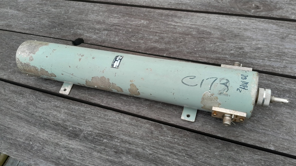
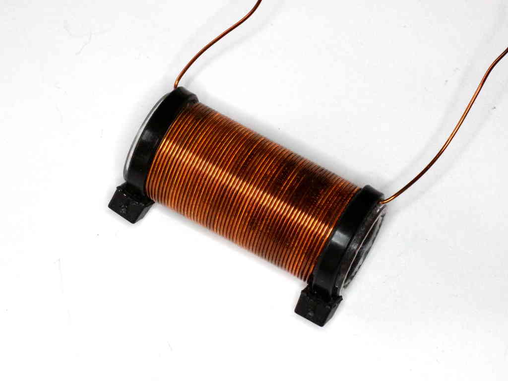
Above is the test inductor, enamelled wire on an acrylic tube, an air cored solenoid.

We speak naively of this sort of component as an inductor, perhaps thinking it is a frequency independent inductance with perhaps some small series resistance. Let me make the distinction, Inductance is a property, Inductor is a practical thing (that includes Inductance… that might be a function of some variables).

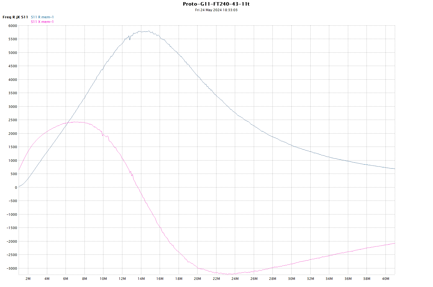
Above is an s11 reflection measurement of the impedance of the air cored solenoid.

Above, focusing below about 5MHz, R is very low and X is approximately proportional to frequency, and the calculated equivalent series L is approximately independent of frequency… so the naive model discussed earlier might be adequate. Measured inductance at 1kHz is 20µH, at 5MHz apparent series inductance is still close to 20µH, but then starts rising, more quickly as the first resonance is approached (see previous plot).

We can calculate a value of shunt C that will resonate the inductor at this first resonance, in this case it is 1.02pF (often referred to as Cse). The parallel combination of 20µH and 1.02pF will have an impedance that is a good approximation of what was measured up to perhaps 1.2 times the frequency of the first resonance, BUT NOT ABOVE THAT. Such an equivalent circuit is useful, be be mindful of the acceptable frequency range.

The existence of higher order resonances shows that this is not simply an inductance. Calculated Cse will not explain the impedance curve much above the first resonance, it will NOT explain higher order resonances.

Understand the nature of the DUT

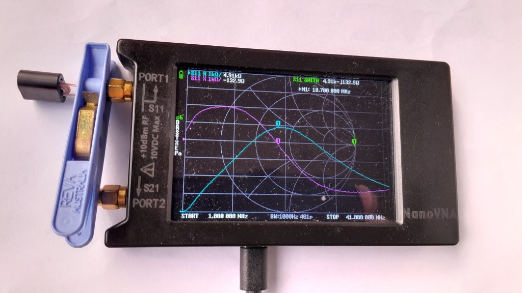
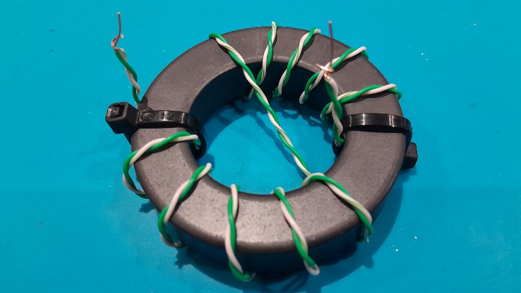
The DUT is a small test inductor, 6t on a Fair-rite 2843000202 binocular core (BN43-202).

We speak naively of this sort of component as an inductor, perhaps thinking it is a frequency independent inductance with perhaps some small series resistance.

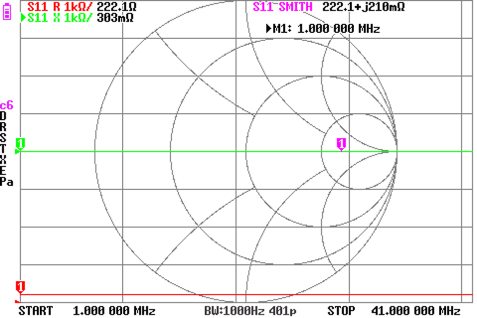
You might look up the Al parameter for the core and calculate its inductance to be \(L=A_l n^2=2200*36=79,200 \text{ nH}\) and calculate its impedance @ 10MHz \(Z=\jmath 2 \pi f L=\jmath 2 \pi \text{ 1e7} \text{ 79.2e-6}=\jmath 4976\).

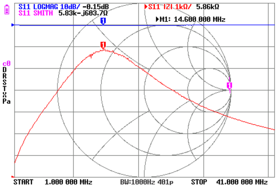
In fact it measures 3206+j1904, so the notion of a fixed inductance with small series resistance is not an adequate model for this component at HF. It exibits a first resonance at about 16.3MhHz.

In fact the DUT is a resonator, plotted here around its first resonance.

Using a ferrite core that is both lossy and frequency dependent permeability might make higher order resonances harder to observe, they are not simply harmonically related and they may be severely damped.
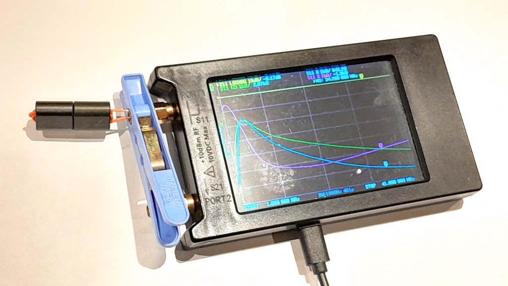
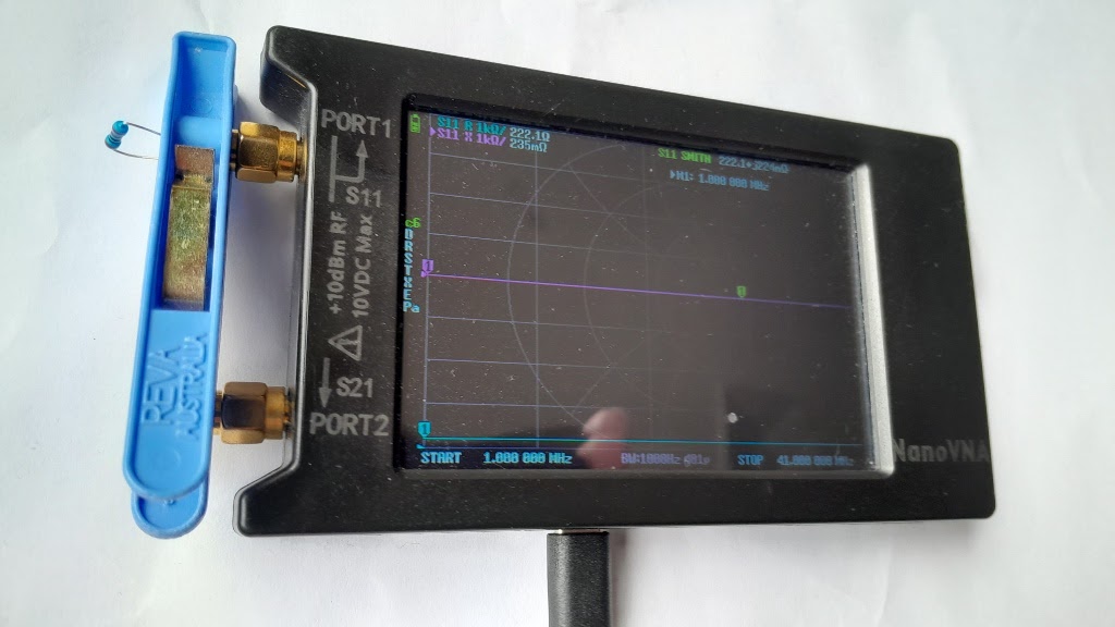
The test fixture

The test uses a small test inductor, 6t on a Fair-rite 2843000202 binocular core (BN43-202) and a small test board, everything designed to minimise parasitics. This inductor has quite similar common mode impedance to a HF good antenna common mode chokes.

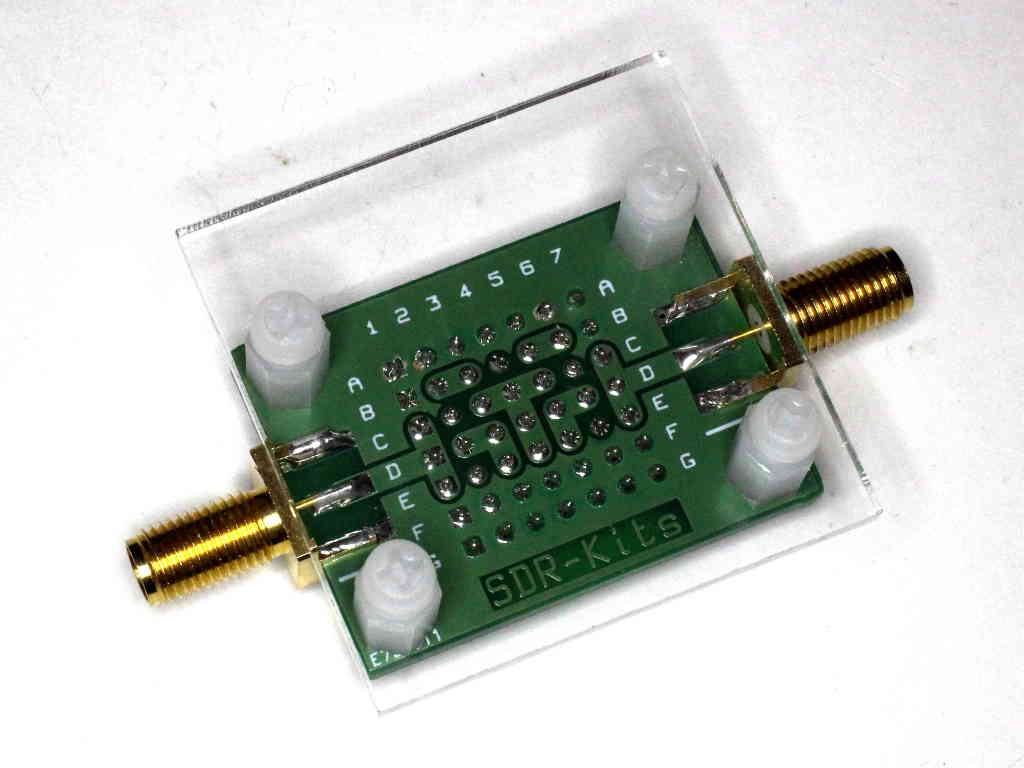
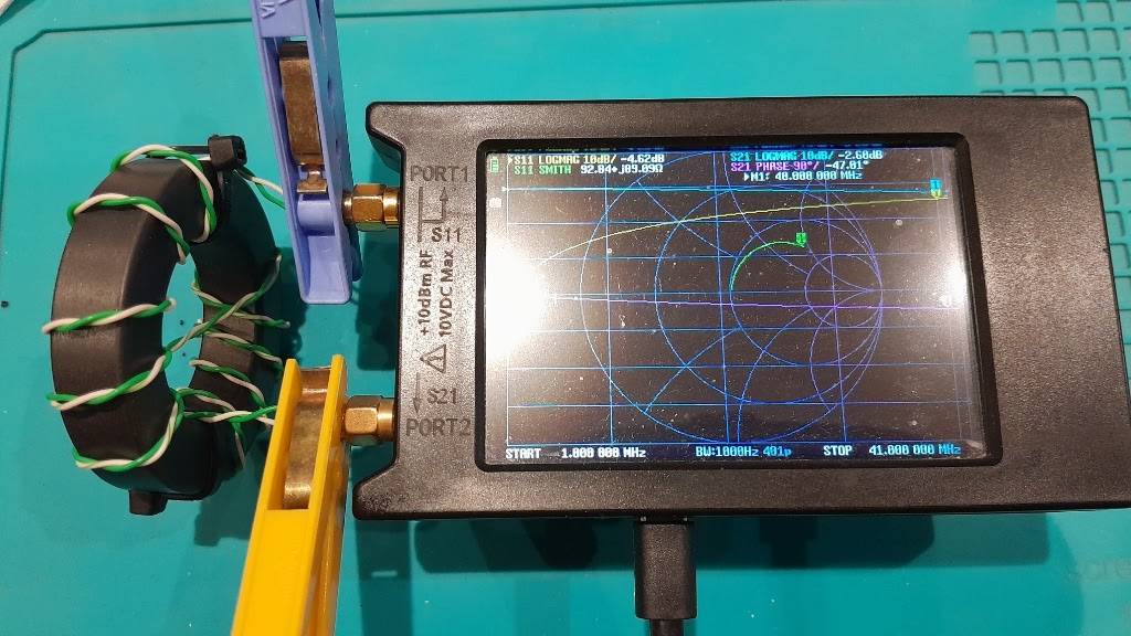
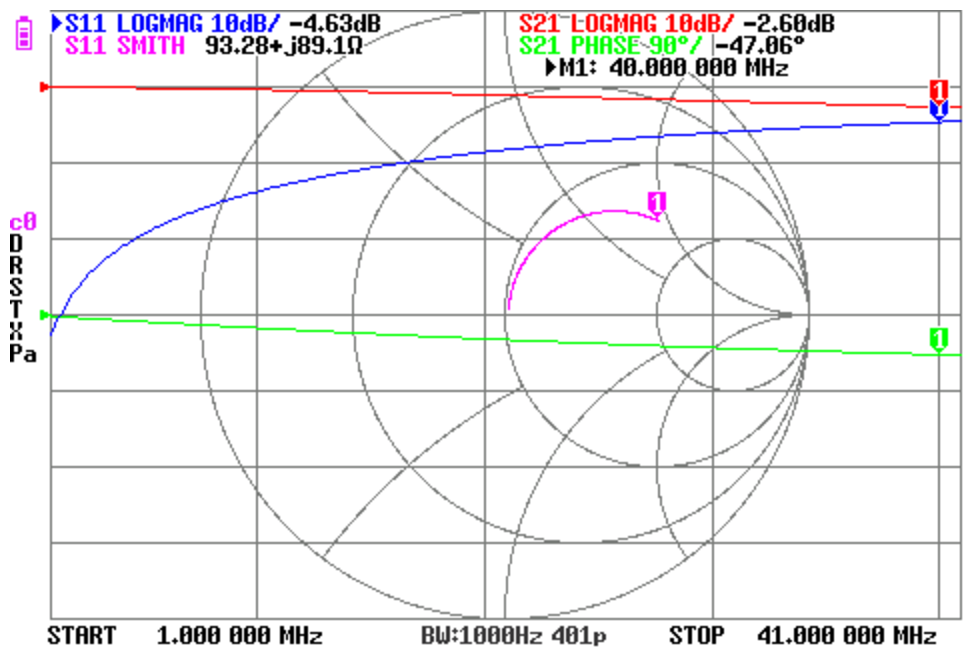
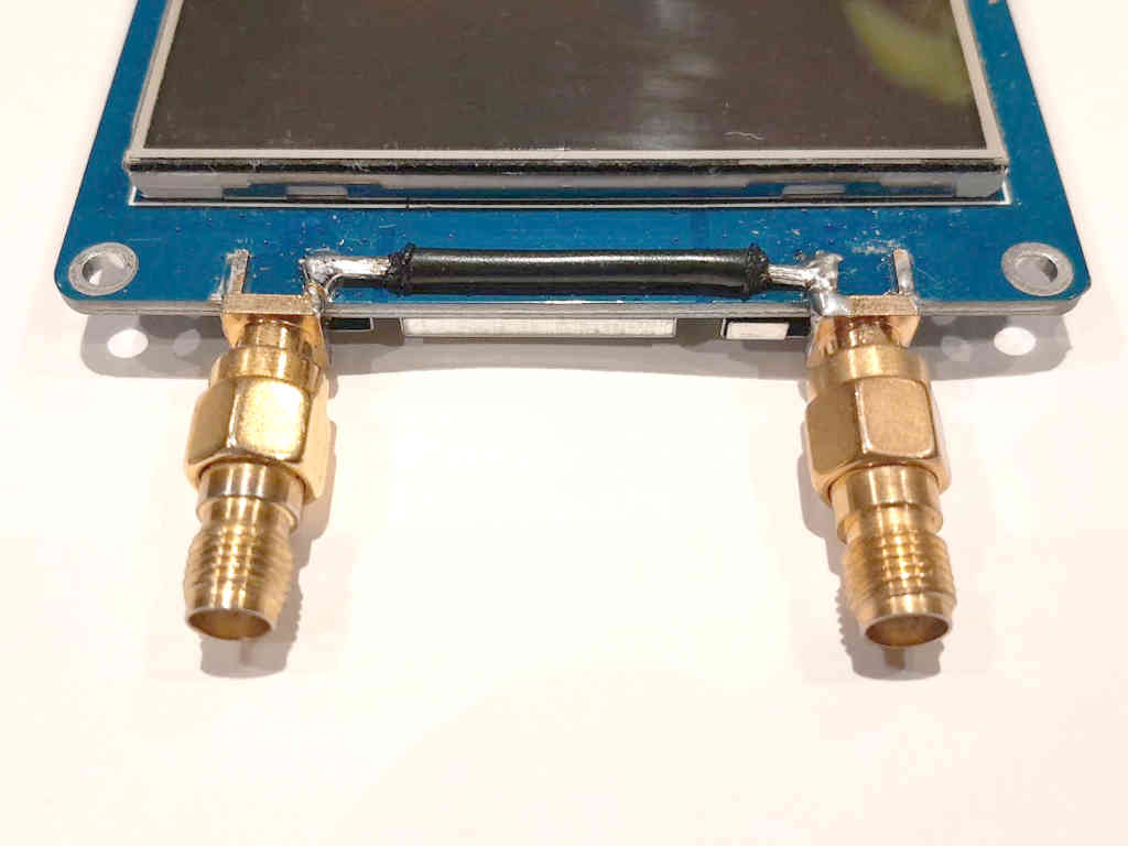
Above is the SDR-KITS VNWA testboard.

The nanoVNA-H4 v4.3 was calibrated using the test board and its associated OSL components. The calibration / correction corrects Port 1 and Port 2 mismatch error. The test board is used without any additional attenuators, it is directly connected to the nanoVNA-H using 300mm RG400 fly leads.

Above, the test inductor mounted in the s11 shunt measurement position.

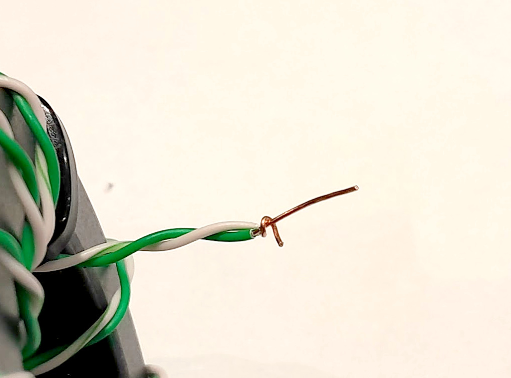
Above is the sub-optimal test setup, the DUT is connected by the green and white wires, each 100mm long.

Measurements and interpretation
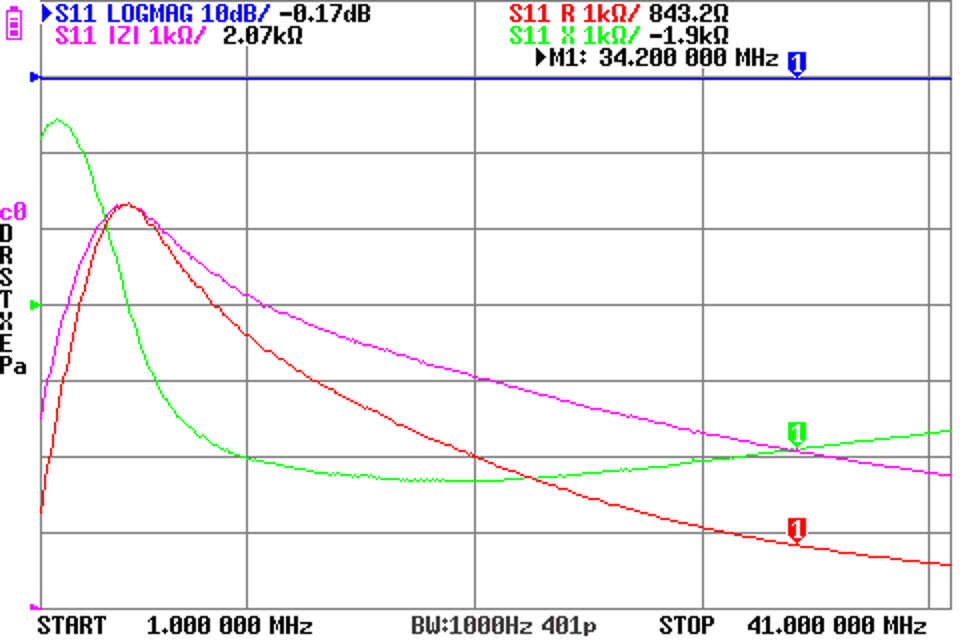
Optimal

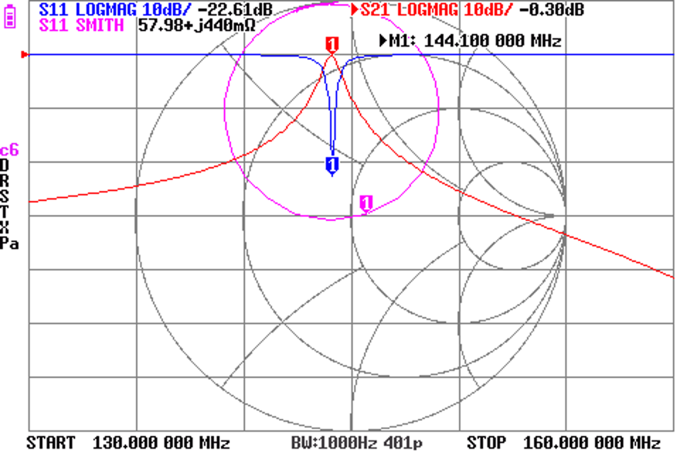
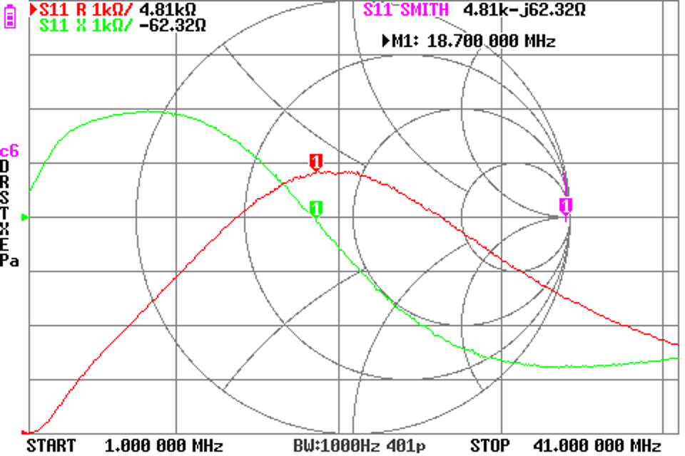
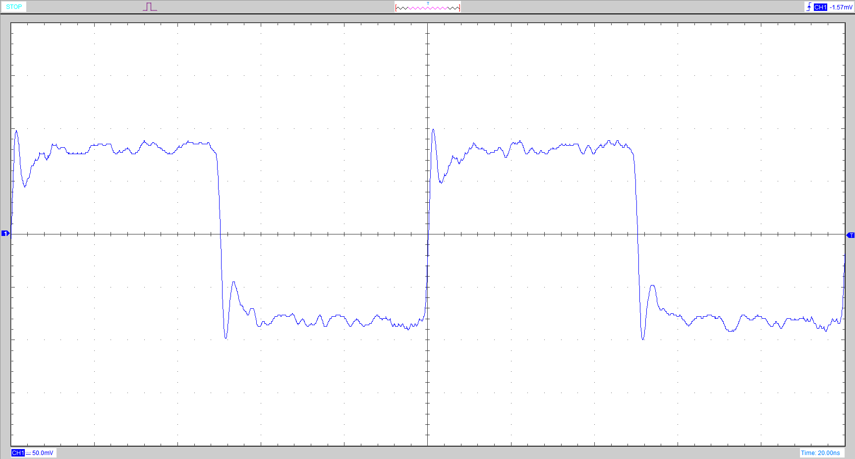
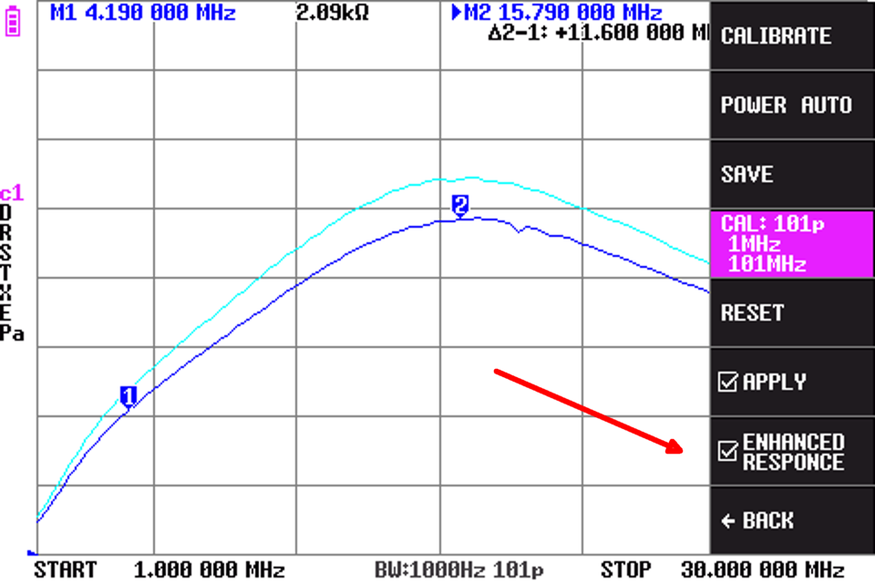
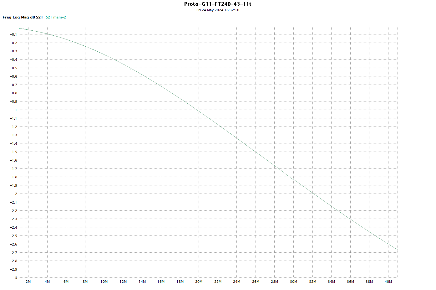
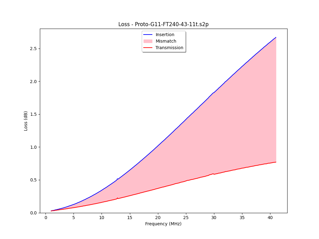
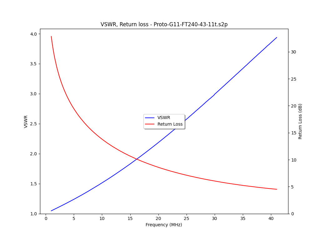
Above are the results of the three impedance measurement techniques.

Note that s21 series through and s21 series pi show no significant difference.

There is a difference between the s11 shunt method and the s21 series methods, the self resonant frequency is slightly different.
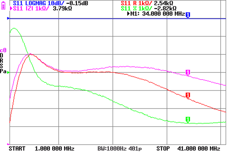
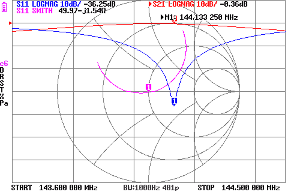
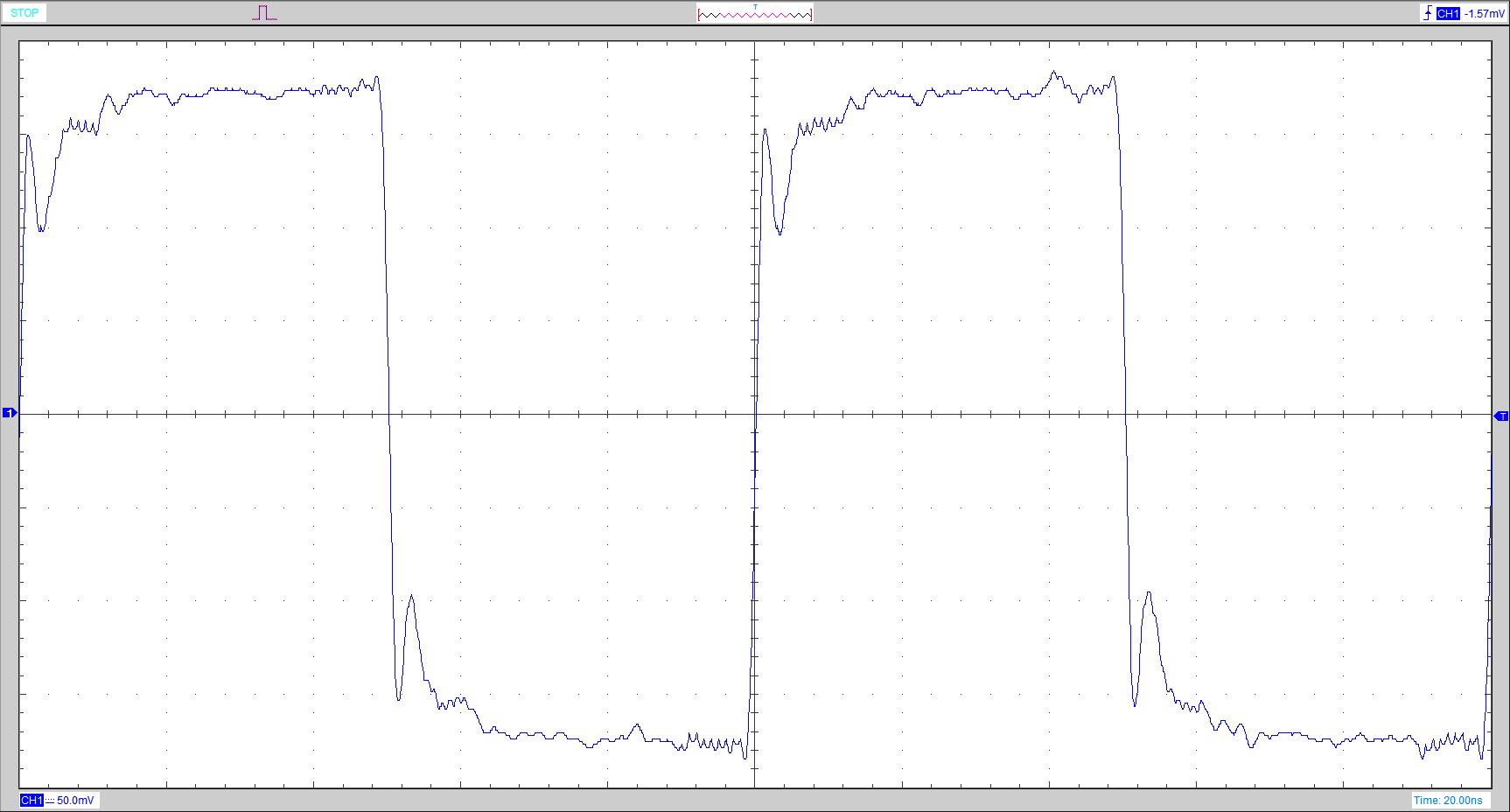
Sub-optimal

It is often held that the series pi or Y21 method corrects a sub-optimal fixture, but if you look closely, the series through and series pi curves have no significant difference between them, and they are only a little different to the plots from the optimal fixture… probably insignificant difference.

Does that mean series through undoes untidy fixtures in general? I doubt it.

Why the difference?

There are differences between the measurement methods, well between s11 shunt and s21 series through though in this case no significant difference from s21 series through to s21 series pi; and differences between the test jigs.

Note the test jig affected one measurement method differently to the other.

The results are sensitive to small changes in fixture layout, temperature, component tolerances etc

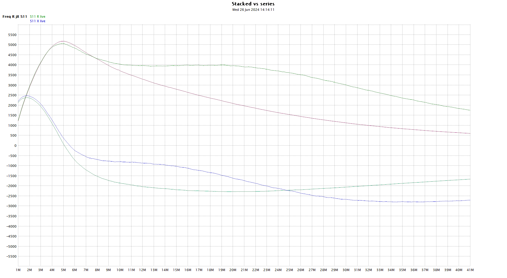
Sensitivity to parasitic fixture capacitance

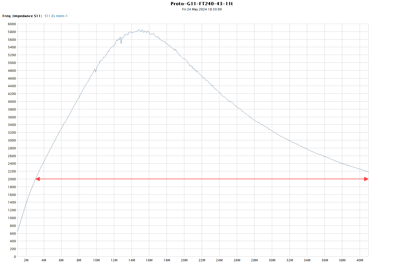
Above is a chart of the measured s11 shunt impedance and two calculated values with 0.2pF of shunt capacitance subtracted and added. Note the effect on maximum R, and the self resonant frequency (SRF) (where X passes through zero).

From this information, we can calculate that the inductor at resonance is represented by some inductance with some series resistance, and Cse=1.5pF. So it is very easy for untidy fixtures, long connections etc to disturb the thing being measured.

BTW, for this DUT that is high impedance around resonance, 6mm of 200Ω transmission line (connecting wires?) has an equivalent Cse if about 0.2pF.

A rule to consider

A good measurement technician challenges his measurements, the fixtures, the instrument etc.

A guide I often give people is this:

if you reduce the length of connections and measure a significant difference, then:

  • they were too long; and
  • they may still be too long.

Iterate until you cannot measure a significant difference.

A challenge to your knowledge

Q: what is the formula for the resonant frequency of a parallel resonant circuit?

What you answer simply \(f=\frac1{2 \pi \sqrt{L C}}\) ?

Practical inductors also have an equivalent series R, and that is not included above… so it is a formula for ideal components, not for the real world.

A: that is the correct formula for a series resonant circuit, no matter how much series R is involved, and it is a good approximation for parallel resonant circuits with high Q, but has significant error for slow Q values (eg single digit.)

Why do I mention this?

Well, ferrite cored inductors may well have Q in the single digit domain, particularly broadband common mode chokes in the region of their SRF.

Last update: 17th June, 2024, 1:20 AM

NanoVNA-h4 v4.3 Return Loss Bridge model, measurement and analysis

By: Owen
14 June 2024 at 09:33

The common resistive Return Loss Bridge discussed the role, characteristics and behavior of an ideal Return Loss Bridge.

Let’s look at the Return Loss Bridge embedded in the NanoVNA-h4 v4.3.

Above is an extract from the schematic for a NanoVNA-h4 v4.3. It includes the source, Return Loss Bridge circuit and detectors. Other NanoVNA versions may have similar implementations, but small differences can have large impact on behavior.

Let’s create a calibrated LTSPICE model of the Return Loss Bridge, source and detector input.

Above is a DC LTSPICE model.

The model assumes that the clock output pin of the si5351A is well approximated by a Thevenin or Norton equivalent circuit, and the output impedance is taken from the datasheet Rev. 1.1 9/18. The datasheet hints that the output impedance is drive level dependent.

Model calcs / measurement

NanoVNA firmware calculates raw S11 as approximately (Va-Vb)/Vs. So let’s tabulate some results from the model for various Zu.

Above are three tables, all are from the model.

Analysis

Note that the the calculated voltage (Va-Vb)/Vs for sc should be -oc, it is not nearly, demonstrating significant departure from symmetry, from ideal. That said, the calculated voltage (Va-Vb)/Vs s11 for the 50Ω load case is quite good.

These values from the model reconcile well with saved sweeps of raw s11 for sc and oc terminations, s11m.

Equivalent source impedance Rth calculated from the model is very close to 50Ω. A load pull test on Port 1 came in very close to 50+j0Ω.

The right hand table compares:

  • the model voltage (Va-Vb)/Vs (which is used by the firmware to calculate raw s11 with (Va-Vb);
  • the reference voltage Vs; and
  • the model bridge unbalance voltage.

Note that:

  • Vs, the reference voltage is load dependent.
  • (Va-Vb) for oc is very nearly -(Va-Vb) for sc, so this is only a small departure from ideal.
  • (Va-Vb) for the 50Ω load is very small, corresponding to raw ReturnLoss=60dB, substantially better than the Vs adjusted case above.
  • (Va-Vb)/Vs for oc is quite different to -(Va-Vb)/Vs for sc,  a large departure from ideal. So, raw s11 is calculated based on a load dependent reference voltage Vs… building significant error into the raw measurements.

Realist that this is a DC model, but will be a good predictor of AC behavior at say 1MHz, things change as frequency increases and there are step changes where each of the harmonic modes are engaged.

The common resistive Return Loss Bridge set out:

Essential requirements of a good resistive RLB:

  1. The source has a Thevenin equivalent source impedance of almost exactly Zref;

  2. three of the bridge resistors are almost exactly Zref; and

  3. the detector is a two terminal load almost perfectly isolated from ‘ground’ and has an impedance of almost exactly Zref.

The NanoVNA-h4 v4.3 fails two of them:

  • the Thevenin equivalent source impedance seen by the bridge itself is not close to Zref (~25Ω); and
  • the detector impedance is a long way from Zref and is not isolated, the grounding of R20 and R21 in the original schematic provides a current path to ground which disturbs the bridge. It is hard to understand why this point is grounded as the bridge output voltage is not balanced, nor is one side grounded, so the load needs to be isolated from ground.

Notwithstanding those problems, it appears the source impedance looking into Port 1 in the simulation happens to be close to 50+j0Ω, and a load pull test supports that, but measurement experience is that there is significant Port 1 mismatch error that needs correction.

These all contribute to less than ideal response report in the model results and saved raw s11 measurement.

The response to this criticism might well be a nonchalant “never mind, VNA error correction will paper over all problems.”

Perhaps… though tests on s21 correction indicate that it does not properly deal with error:  An experiment with NanoVNA and series through impedance measurement… more.

That article has inspired review of s21 correction, and Enhanced Response Correction has been added to NanoVNA-D v1.2.32  by Dislord, and it has significantly improved s21 measurement accuracy.

Last update: 14th June, 2024, 7:33 PM

Measurement / evaluation of an RF filter response with NanoVNA – with ERC

By: Owen
14 June 2024 at 00:12

Measurement / evaluation of an RF filter response with NanoVNA gave an example measurement of a low pass filter.

Above is a plot of |s11| and |s21| from the article.

This article remeasures the filter with and without Enhanced Response Correction (ERC) in the VNA.

Let’s talk about the VNA for a moment…

The measurements were made with NanoVNA-H4 v4.3 and Dislord’s NanoVNA-D firmware v1.2.30.

At An experiment with NanoVNA and series through impedance measurement and An experiment with NanoVNA and series through impedance measurement… more I discussed inaccuracy of the combination for that type of measurement.

The problem raised was demonstrated with series though impedance measurement of a known 200Ω resistor, and the error was quite significant. Similar error might be expected for series though impedance measurement of a common mode choke.

The problem is due to uncorrected source mismatch error, and will have most effect when the DUT presents a significant mismatch to Port 1. The series though impedance measurement and shunt though impedance measurement will both be susceptible, as will DUT such as filters in the reject regions where InsertionVSWR is high, but less so in the pass region where InsertionVSWR is low.

An issue was raised as IMHO it was not a very difficult thing to implement (I had prototyped it in NanoVNA-App). Within days Dislord had coded a solution which implemented ERC, and it works very well, it is in NanoVNA-D firmware v1.2.32.

Impact of source mismatch error

The series though impedance measurement and shunt though impedance measurement will both be susceptible, as will DUT such as filters in the reject regions where InsertionVSWR is high, but less so in the pass region where InsertionVSWR is low, or any other DUT that presents high InsertionVSWR to Port 1.

200Ω

A s21 series through measurement of the 200Ω SM 1% resistor was conducted and results were very close to the measured value of the resistor.

A subtle point lost to those who rate series through impedance measurement over s11 reflection measurement is that ERC depends on corrected measured s11.

Low pass

This repeats the measurement of the filter at Measurement / evaluation of an RF filter response with NanoVNA, freshly recalibrated and measured (the filter is susceptible to temperature change).

Above is a comparison of measurements (corrected in the NanoVNA) with and without ERC, green is with and magenta is without. At 14.09MHz, the ERC trace shows approximately 1dB lower |s21|, ie 1dB more rejection, 80% of the power output.

Load mismatch error

Load mismatch error is at this time uncorrected, so it remains important that the load is very close to 50+j0Ω for good s21 accuracy.

Some of the NanoVNAs have quite high ReturnLoss on Port 2, some are mediocre and warrant a good external attenuator to improve it.

A common way in which people compromise Port 2 ReturnLoss is the measurement fixture… measure it through the fixture to check.

Conclusions

Whilst ERC might seem insignificant in some scenarios, in others it might be quite significant. The series through measurement techniques warrant ERC.

Last update: 14th June, 2024, 10:12 AM

Don’t Cha Know What June Is? Band Pass Filter Season!

By: KM1NDY
13 June 2024 at 09:51

With ARRL Field Day around the corner, it is the time of year where amateur radio operators far and wide wonder if they are going to be stuck having their QSOs wiped out every time their neighbor keys up the microphone. Interference between stations in a multi-transmitter field day operation can be the norm if you didn’t think to use band pass filters.

So out my stash of little gray metal boxes came, and I began checking their VSWRs for a down-‘n’-dirty pre-Field Day check-a-roo…

I don’t love the VSWR trace of this 6M filter, but it will probably suffice for Field Day, where I plan on setting up a 6M 4-element beam, and operating largely on FT8 to try to intercept the “Alpha” stations that are trying to rack up the “Free VHF station” points. That, and when else do I get to put up my 6M yagi???? FT8 is operated on 50.313 MHz which should have a VSWR under 1.2.

These Array Solutions elliptic filters have a beautiful looking VSWR. I really wish I had spent my ham bucks acquiring a full set of these. Apparently Array Solutions is not making them anymore, but a company called Hamation is? Oh, and for anyone not familiar with the RigExpert Antenna Analyzer (1-port VNA), the blue portion of the display indicates the ham band with frequency along the horizontal access and VSWR on the vertical access. Keep in mind that the VSWR we want is as close to 1 as possible!

Now 12M is a WARC band of course, meaning you cannot use it for contesting. In general, it is second only to 60M as my least used band. But, boy, that band pass filter looks great!

I expect 15M to be hopping on Field Day. I am glad this filter looks good.

Another WARC band, i.e. Field Day no-go… But a good looking filter!

Now 20M. Let’s just say I am not at all happy with this filter. Granted, it has probably been heavily abused over its several years now with me. Dunestar has gone out of business since August of 2023. Their original owner became a silent key right around the time that I purchased this set. I decided to try out Morgan Systems Surestop bandpass filters for 20M and 40M for this year’s Field Day. You’ll notice the 40M filter looks reasonable, but when actually under use, the VSWR seen at the transceiver is often high. And we can’t be without a highly functional 20M and 40M stations when it comes to Field Day operations. We will see how the Surestop filters behave…

The 30M filter looks superb! Of course, there is no operating 30M on Field Day.

The 40M filter looks a bit janky. Technically, it should function okay. But like I mentioned, this filter often creates a high SWR at the transceiver. I have a replacement here for it now.

Ugghh. The 80M filter is downright scary looking. I probably should have replaced it when I had a chance.

The top band filter isn’t great. What else can I say? I am not sure I ever even used this filter on 160M. I do think I will slowly start replacing my filters with one of the other manufacturers with time. Although I am grateful to have been able to get a set of Dunestar filters, especially since they provided a boatload of good multi-operator experiences over the years, the older and wiser me wishes I had put my money elsewhere.

Here are the “guts” of one of the Array Solutions 3rd order elliptic filters. Note the interesting use of a hot glue like substance to hold the windings in place, the beefy size of the enameled wire, and the use of ceramic capacitors. Silver-Mica capacitors are often recommended for use in band pass filters

…and a representative schematic from this excellent LC Filter Design calculator by Marki Microwave

Now we can contrast the design and construction of the Array Solutions band pass filter with the 2nd order Dunestar bandpass filter (below). This design consists of two airwound coils and capacitors mirroring and shielded from each other on the input and output side.

Every time I get around to thinking about, testing, and opening up my band pass filters, I can’t help but think: It would be so much better to make these myself. For some reason, this does not seem to be an area that has been overly tackled by hams. In fact, there is really only one prevailing design by Lew Gordon K4VX, a 3rd order Butterworth filter, that is well-described and seems easy-ish to reproduce by the average everyday ham (i.e., one that does not design RF products for a living). The W3NQN band pass filter design article is a much more complex document to follow.

I have dabbled in making band pass filters before, but have found myself hindered by the testing process. I since learned to use the “low Z” setting of my oscilloscope. So, once I again, I found myself constructing an ugly little device, this time a low-power 160M version of K4VX’s Butterworth filter. The schematic, construction, and component values are all documented in the article. This is nothing more than a capacitor (~4000 pF) and inductor (~2.2 µH) connected in parallel on the left hand side as well as a capacitor (~4000 pF) and inductor (~2.2 µH) connected in parallel on the right hand side, with another capacitor (~400 pF) and inductor (22 µH) in series in the middle connecting the two sides. I just soldered everything together and attached it across VHF connectors.

And although the Marki Microwave design tool proposes different capacitor and inductor values for its version of the 160M 3rd order Butterworth band pass filter, you can still get an idea of what the schematic, and scatter plot parameters (insertion loss and return loss) of the filter should look like.

The first test I performed with the band pass filter was pass a sine wave through it from below the 160M band (which spans from 1.8 MHz to 2 MHz). I started with 500 kHz and passed the signal into my oscilloscope, making sure to turn on the low impedance (50 ohm) setting.

I did indeed have a fairly weak signal.

When I increased the signal generator frequency so that the waveform outputted was within the pass band of the filter (1.8 MHz), the oscilloscope showed a much larger voltage. Keep in mind that it is Channel 2 (“CH2”, the bottom box!), that you want to be looking at on the signal generator if you are following along with the pictures.

There is no change to the oscilloscope settings between the 1.8 MHz input (below) and the 500 kHz input (earlier). Clearly the voltage recovered at the 1.8 MHz setting is much larger.

Now to take a look at the NanoVNA results. The filter was simply placed between port 0 and port 1 of the NanoVNA. The vertical gray bar represents the frequency range of the 160M ham band. The filter I constructed did not use components of the exact values recommended in the K4VX article, thus the reason the filter performs at a lower frequency than expected.

Regardless, you can see below that the shape of the S11 (return loss) and S21 (insertion loss) parameters are very similar to that predicted by the Marki calculator. My filter is below:

And, again, the S11 and S21 parameters as predicted by the Marki calculator:

Well, there you have it. Band pass filter season! Field Day is almost here, and we are going to go with what we have. However, my mind has been spinning around the idea of constructing my own band pass filters so that I can more easily fix and replace the rather fragile devices as needed. And although this was a tiny little experiment, I think it shows that these band pass filter designs are indeed reproducible with accuracy. Will a KM1NDY band pass filter design show up here in the near future?! The Magic 8 Ball says “Reply Hazy. Try Again Later”!

Catchya on the flippity flip!

KM1NDY

An experiment with NanoVNA and series through impedance measurement… a fix

By: Owen
12 June 2024 at 22:11

An experiment with NanoVNA and series through impedance measurement… more concluded with:

The NanoVNA-H4 v4.3 NanoVNA-D v1.2.30 using 5 term calibration does not appear to give good accuracy on series through measurement of impedance.

Further investigation identifies several possible contributions, the main one being the s21 correction algorithm and implementation.

Dislord confirmed that the s21 correction algorithm did not include Enhanced Response correction, and has released v1.2.32 which includes the feature (which has to be enabled on the calibrate menu).

Note the E in the cal status column at left.

The nanoVNA-H4 v4.3 with Dislord v1.2.32 was calibrated using a SDR-kits test board and its associated OSL components. The test board is used without any additional attenuators, it is directly connected to the nanoVNA-H4 using 300mm RG400 fly leads.

Test inductor

The test inductor gives a small DUT that has similar characteristics to a HF common mode choke.

Above, the test inductor mounted in the s11 shunt measurement position, but the tests below are in the s21 series through connection.

Above is a plot of |Z| from 1 to to 30MHz without Enhanced Response correction.

Above is a plot of |Z| from 1 to to 30MHz with Enhanced Response correction, and the without case shown in cyan for comparison. In this case the non ERC trace is inflated about 10%.

Above, it is interesting to compare three methods of impedance measurement. The series-π method is often known as the K6JCA Y21 method.

200Ω

A s21 series through measurement of the 200Ω SM 1% resistor was also conducted and results were very close to the measured value of the resistor.

Conclusions

The NanoVNA-H4 v4.3 using 5 term calibration does not appear to give good accuracy on series through measurement of impedance unless Enhanced Response correction is enabled (Dislord NanoVNA-D v1.2.32 and later).


Last update: 14th June, 2024, 2:42 PM

NE6F’s common mode current tester – Part 2

By: Owen
30 May 2024 at 23:35

NE6F’s common mode current tester – Part 1 ended with the following:

Common mode current adjacent to a small choke

Consider a straight section of coaxial feedline not close to other materials, and with a small common mode choke inserted in the feedline. A “small” choke means one that is a very tiny fraction of a wavelength, say λ/100, from connector to connector.

Q1: Ask yourself that if say 1A of common mode current flows into one connector, what is the common mode current at the other connector?

Q2:What is your answer if you were told the balun was specified to have a CMRR of 20dB?

The answer to Q2 is relatively easy, CMRR is not a meaningful statistic for a common mode choke deployed in a typical antenna system, it would not change the answer to Q1.

The answer to Q1 needs a longer explanation… let’s do it!

Common mode current distribution is almost always a standing wave.

Above is a plot of current distribution of an example dipole antenna system with coax feed. The dipole is slightly off centre fed to drive a significant common mode current on the vertical coax feed  which is grounded at the lower end.

Note the standing wave on the vertical section, it has maxima and minima (if it is long enough), and these are unrelated to possible standing waves inside the coax, ie in differential mode.

Note that if we took spot measurements of the magnitude of common mode current |Icm| at points A, B and C we would get different results.

Broadly, Icm changes relatively slowly over a small electrical distance (say λ/100), except near deep minima if they exist.

Above is the same model with a common mode choke inserted near ground. Note that it has changed the magnitude and distribution of Icm, and more importantly, note that |Icm| at both ends of the choke are very similar, and in fact slightly lower on the antenna side of the choke.

If you make spot measurements either side of an electrically short (say length<λ/100), you will not usually find a large difference… except in the region of a current minimum.

The common notion that |Icm| is much lower on the tx / ground side of the choke is deeply flawed, and even worse is to think that CMRR can be used to calculate the reduction.

NE6F’s video of measurement of his balun’s effectiveness.

N6EF demonstrates measurement with his dual probe meter asserting that “this choke is doing a pretty good job,” but is the measurement a valid basis for that assertion?

Above is a capture from the video with my added notations of four currents, I1-4.

Having set his instrument to read 100% of scale on the Port A probe, he switches to display the Port B probe.

Above. a stunning drop, it is reading perhaps <1% of scale on Port B. Some might infer that proves CMRR>40dB.

Let’s look at that test setup again.

Above is a capture from the video with my added notations of four currents, I1-4.

NE6F demonstrates that I4 is less than 1% of I1 (though the meter response may not be linear at low readings).

Now look at the conductive bulkhead and the bulkhead adapter which connects the coax shield to the bulkhead. At this point a circuit node with three conductors is formed and currents annotated:

  • I1: shield from the antenna side;
  • I2: bulkhead conductor; and
  • I3: shield to the choke.

The measurement made ignores the presence of current path I2, and so all conclusions are invalid.

With the information given earlier, you might well think that it is likely that I3 is approximately the same as I4 (measured at <1% of I1), and that I2 is probably almost the same as I1, ie that this shunts, diverts common mode current on the antenna feed line to ground. That might be an effective measure in preventing ingress to the equipment cluster, but it does not reduce Icm on the main feedline or the undesirable effects of that.

Of course that is just supposition… but it should drive measurement of |I3| to better infer |I2|.

Homework

Make or buy an effective common mode current meter, and make some measurements adjacent to a common mode choke to test your understanding of what it does or does not do.

Last update: 1st June, 2024, 2:54 PM

Baluns: you can learn by doing!

By: Owen
25 May 2024 at 05:23

This article presents a simple way to make measurements of a prototype Guanella 1:1 current balun, measurements that can guide refinement of a design.

The usual purpose of these transmitting Guanella 1:1 current baluns is to reduce common mode feed line current. Not surprisingly, the best measure of a device’s effectiveness is direct measurement of common mode current (it is not all that difficult), but surprisingly, it is rarely measured.

Above is the prototype transformer being a Fair-rite 5943003801 (FT240-43) wound with 11t of solid core twisted pair stripped from a CAT5 solid core LAN cable and wound in Reisert cross over style. Note that Amidon #43 (National Magnetics Groups H material) is significantly different to Fair-rite #43.

There is no need to wind a prototype using expensive materials, the measurements made with the above prototype are very useful in guiding development without wasting expensive materials. Further, the measured results are very close to the behavior of the ‘raw’ balun.

s21, s11 measurement of through transmission


Above is the configuration for the through test, the clothes pegs are used to clamp one conductor to the outside of the SMA jacks, the inner wire is poked into the inner pin, the VNA is sitting on a cardboard box, the whole thing is on a wooden table. An alternative to the clothes pegs are small zip ties.

Above is a screenshot from the NanoVNA of the through measurement. The relevant traces are s11 Logmag, S11 Smith, and S21 Logmag.

Above is an expanded graph of |s21|. At first glance, you might be horrified by the value of -1.8dB @ 30MHz. Many would assert that this shows a loss of 1.8dB… but more correctly it is InsertionLoss of 1.8dB and conversion of RF energy to heat is likely to be less.

See Measurement of various loss quantities with a VNA for discussion of Loss terms.

Above is a graph disaggregating InsertionLoss into (Transmission) Loss and MismatchLoss. Thicker conductors will have less Loss, and would be used in practical baluns.

Above is a graph showing InsertionVSWR wrt 50Ω and ReturnLoss wrt 50Ω.

The significant mismatch is due to the fact that the balun introduces about 800mm of transmission line with Zo around 100Ω.

If you want low InsertionVSWR wrt some reference Zo, then the transmission line (the twisted pair or coax) needs to be that same Zo.

Is the InsertionVSWR and associated impedance transformation a problem? Well if you are using an ATU, it should not matter, and imperfection is dealt with by the ATU.

s11 reflection measurement of Zcm

Above, the DUT was reconfigured for Zcm measurement by twisting the white wire around the green wire at each end to bond them, leaving a short straight section of the green wire for connection. One end is inserted into Port 1 jack inner, the other was clamped to the male threads of Port 2, ie grounded.

Note: my NanoVNA-H4 has been modified by addition of a short direct wire between the ground side of Port 1 and Port 2 jacks inside the case (see above).

(If wound with coax, Zcm measurements are made between shield ends, ignore the inner conductor.)

Above is a screenshot of the Zcm measurement, |Zcm| peaks at about 14.6MHz.

Above is a plot of |Zcm| taken from the .s1p file saved during measurement. |Zcm| > 2000Ω from 3MHz to more than 40 MHz.

Above is a plot of the R and X components of Zcm taken from the .s1p file saved during measurement.

Above is a plot of the ReturnLoss taken from the .s1p file saved during measurement.

Above is a plot of the InsertionVSWR taken from the .s1p file saved during measurement.

Conclusions

Good / valid measurements of a prototype Guanella 1:1 balun can easily be made with a NanoVNA using low cost materials in capable hands.

Keep in mind that you are measuring a sample of one or a small number and that ferrite has a wide tolerance specification, and is temperature sensitive.

Experimenting with measurement setups and prototypes is the beginning of understanding of these things, more so that soaking up the utterings of armchair experts.

Go build and measure some prototypes, try different cores, different turns, different winding layouts, twisted / untwisted / coax etc.

Downloads

Proto-G11-FT240-43-11t.7z

Last update: 31st May, 2024, 5:28 AM

Velocity factor measurement

By: Owen
18 May 2024 at 08:41

A frequently asked question is how to measure transmission line velocity factor. The wide adoption of the NanoVNA has spurred these questions.

So, it is good that ownership of a NanoVNA stimulates thinking and search for applications of the instrument.

I note that when these questions are asked online, early responses include recommendation of using the VNA to perform a TDR transform to measure the electrical length of the cable and calculate the velocity factor as \(vf=\frac{\text{PhysicalLength}}{\text{ElectricalLength}}\). The resolution of the NanoVNA swept from 1 to 1500MHz with 401 steps is around 60mm, so you can only measure to about 0.25% resolution if you have a test cable 20m long. So this method might not be very practical in a lot of situations for that reason alone. More later…

It is practical to measure the quarter wave resonance of a shorter section of test cable to better than 0.1% resolution.

A significant problem measuring short cables is the contribution of the test fixture, the reference plane is usually not at the very beginning of the uniform cable, if you know where that is anyway (it may be inside a connector).

Let’s look at an example, a measurement of some ordinary nominally 300Ω TV windowed ribbon line.

Above is the test fixture, the VNA and 1:1 transformer board have been OSL calibrated to a point very close to the pins of the grey terminal block. The transformer module is described at Conversion of NOELEC style balun board to 1:1.

A section of line that measured 0.303m from the grey terminal block to the end of the line was measured observing phase of s11, and the frequency where phase switched from -180° to 180° noted as 209.000MHz, see above. We can calculate the electrical length as c0/fo/4=0.3586m and vf=0.845.

That went well, let’s try a longer section.

A section of line that measured 1.750m from the grey terminal block to the end of the line was measured observing phase of s11, and the frequency where phase switched from -180° to 180° noted as 37.115MHz, see above. We can calculate the electrical length as c0/fo/4=2.019m and vf=0.867.

Why do they disagree?

The problem is that the length measurements made are not from the reference plane, it is somewhere towards the VNA, and in fact both sections are physically a little longer.

We can use Velocity factor solver.

Above is the solution, the distance measurement zero point (the outer edge of the grey terminal block) is in fact 36.18ps (9.45mm) from the reference plane.

The final solution is good to 0.1% of velocity factor (pu).

What about the nanoVNA ‘measure cable’ facility?

From this and the measured length of 1.750m we can calculate VF=1.75/2.073=0.844. The 3% error is attributable to the error in length measurement datum and reference plane. The error will be worse for a short cable section, less for a long cable section.

What about the nanoVNA TDR (FDR) facility?

Above is a sweep 1-1500MHz with 401 steps and VF set to 100%. Range resolution is about 78mm in free space, more like 68mm for this cable for maximum cable length of 31m in free space, more like 27m for this cable.

So, we measure the first impulse peak at 2.109m. From this and the measured length of 1.750m we can calculate VF=1.75/2.109=0.829. The 5% error is attributable to range resolution and the error in length measurement datum and reference plane. The error will be worse for a short cable section, less for a long cable section.

Parting thoughts

Some parting thoughts:

  • popular alternatives are not as accurate as often believed;
  • velocity factor is not independent of frequency, though it is approximately so for most good RF cables above about 10MHz;
  • most applications are not as phase critical as believed;
  • many if not most measurements I see described online give questionable results;
  • solid dielectric coax cables are usually very close to datasheet, and results otherwise are questionable;
  • foam dielectric coax cables do have significant variation (due to variation in gas content) and warrant accurate measurement for phase critical applications; and
  • two wire lines pose a challenge with used with an ‘unbalanced’ instrument, and workarounds proposed are often troublesome.
Last update: 20th May, 2024, 12:00 AM

Measurement / evaluation of an RF filter response with NanoVNA

By: Owen
17 May 2024 at 22:15

One sees questions online about measuring a filter response using the NanoVNA.

Let’s discuss filters, the DUT, for a moment.

Filters are usually designed to operate with a given source impedance and given load impedance. It affects the response, and measuring a filter with different source and load impedance that it was designed for, or specified in a test procedure gives invalid results.

This article gives an example measurement of a low pass filter designed for a 50Ω system. The filter is designed for harmonic suppression from a transmitter on the 40m ham band (7-7.2+MHz).

We are interested in measurement of the filter as a two port device.

The VNA as a two port test instrument and suited to measurement of this filter because the impedances match.

Above is a block diagram of the signal flow in a two port test with a VNA. An incident wave (Vi) from Port 1 is partially reflected at the DUT input (Vr), and partially transmitted by the DUT to Port 2 (Vt). We make the assumption that there is zero reflection at Port 2 (ie that Port 2 input impedance is 50+j0Ω… though that might not be a very good assumption with low end VNAs… measure it).

Specifically, VNA measurements expressed as S parameters are:

\(s_{11}=\frac{V_r}{V_i}\); and

\(s_{21}=\frac{V_t}{V_i}\).

S parameters are complex quantities, they can be expressed in polar form (magnitude and phase) or rectangular form (real and imaginary parts).

Often just the the magnitude is of interest, and it is often expressed in dB.

Other interesting metrics can be derived:

  • \(ReturnLoss_{dB}=-|s_{11}|_{dB}\); and
  • \(InsertionLoss_{dB}=-|s_{21}|_{dB}\).

Test configurations

The filter designer may specify one of two common methods of measurement and lineup of filters (or both):

  • transmission measurement / lineup; and
  • reflection measurement / lineup.

Transmission measurement / lineup

\(|s_{21}|_{dB}=20 \log \frac{V_t}{V_i}\). If the network input impedance is approximately 50+j0Ω, the then \(Gain_{dB} \approx |s_{21}|_{dB}\) and \(TransmissionLoss_{dB} \approx -|s_{21}|_{dB}\).

See Measurement of various loss quantities with a VNA for discussion of cases where input impedance is not very close to 50+j0Ω.

So, lineup instructions might be to adjust to a specified response shape.

Reflection measurement / lineup

Reflection measurement specifications might stipulate a response in terms of ReturnLoss vs frequency.

An example low pass filter (LPF)

The example LPF is one sold by Sotabeams as a transmitter filter in a 50Ω system for the purposes of harmonic suppression, this one is their 40m filter. My own intended use is between 7.0 and 7.2MHz, let’s call that the band of interest (BOI).

Let’s firstly look at plots based on magnitude of s11 and / or s21.

Above is a plot of |s11| and |s21|. Note that |s21| falls off above about 7.2MHz.

Above is a zoomed in plot of |s11| and |s21| in the 40m band. InsertionLoss (|s21|) is quite low ‘in-band’, and less than 0.21dB over the BOI.

Above is the same plot with the  |s11| statistic selected for the marker display. |s11| is moderately low, <-20dB over the BOI.

NanoVNA does not (currently) display ReturnLoss, above is a plot of in-band ReturnLoss from NanoVNA-App.

Above is a plot of in-band InsertionVSWR from NanoVNA-App. InsertionVSWR is moderately low, <1.26 over the BOI.

As explained at Measurement of various loss quantities with a VNA InsertionLoss can be disaggregated into to interesting components, InsertionLoss=MismatchLoss+TransmissionLoss. (TransmissionLoss is simply Loss, but let’s use the term TransmissionLoss for clarity in this article.)

Above is a disaggregation of InsertionLoss into its components over the frequency range 2-15MHz It can be seen that whilst MismatchLoss is quite small below the filter cut off frequency, it becomes quite high in the reject frequency range.

Above is a disaggregation of InsertionLoss into its components over the frequency range 6.9-7.5MHz.

In the BOI, InsertionLoss is less than 0.21dB. TransmissionLoss is less than 0.18dB, which allows us to calculate the heat lost with say 10W input power as \(P_{loss}=P_{in} (1-10^\frac{\text{-TransmissionLoss}}{10})=0.406 \text{ W}\).

Now to phase interpretation.

For some applications, phase response is important. Most commonly, where phase is important, one wants propagation time or delay through the filter to be independent of frequency so that complex waves are not distorted by delay to some frequency components. Constant delay or propagation time means phase proportional to frequency, \(Phase \propto Frequency\).

Above is a plot of phase of s21 vs frequency, it is not quite linear, not quite proportional to frequency. A better way to view this is showing GroupDelay (which NanoVNA’s menu tends to call Delay).

Above is a plot of phase of GroupDelay of s21 vs frequency. For a phase linear filter response, GroupDelay would be approximately constant. The response of a filter with critical phase linearity might be specified as limits on GroupDelay over the ‘in-band’ frequency range.

Traps with the NanoVNA and like

The signal emitted by Port 1 may not be a pure sine wave, but a squarish wave. In CW mode where sweeping is suspended, the output is probably not a pure sine wave (as implied by the industry term CW meaning continuous unmodulated sine wave). Hams give a different meaning to CW, and NanoVNA another meaning again.

If the output signal is a complex wave, broadband detectors as often used with Standard Signal Generators and conventional Sweep Generators are not suitable for measurements.

Some kinds of filters require a larger dynamic range than the NanoVNA, eg a repeater duplexor for which you might want to measure rejection notches of over 100dB.

If the filter is not entirely passive, then the output level from the VNA becomes relevant in terms of overload and possibly any form of automatic gain control.

Legacy test setups

50Ω Sweep generator with 50Ω crystal detector

The sweep generator generates a nearly pure sine wave.

The detector (eg HP-423A)  terminates the DUT in 50Ω and provides Y voltage to an oscilloscope, the X voltage coming from the sweep generator or possibly the oscilloscope’s internal timebase synchronised to the sweep generator. Detectors often produced a -ve voltage, and the trace on the oscilloscope was  ‘right way up’ for gain display.

A VNA may be substituted depending on level requirements, Port 2 provides the 50Ω termination.

50Ω Sweep generator with high impedance detector

The sweep generator generates a nearly pure sine wave.

The detector is high impedance and does not load the filter, so the filter must be loaded with its design load. The detector provides Y voltage to an oscilloscope, the X voltage coming from the sweep generator or possibly the oscilloscope’s internal timebase synchronised to the sweep generator.

It may be possible to design and build a high impedance buffer amplifier (eg FET source follower followed by a BJT emitter follower ahead of Port 2 to make a high impedance probe which will give similar results to the high impedance detector discussed above.

Last update: 5th June, 2024, 5:03 AM
❌
❌