Normal view

There are new articles available, click to refresh the page.
Before yesterdayMain stream

How to troubleshoot a jumper wire

By: Dan KB6NU
4 July 2024 at 18:28

Tuesday, my friend Paul, KW1L, texted me, and asked if I could come over to his house and help him with his new antenna. He had just purchased and installed a Cobra Ultra-Lite Junior, and he didn’t think that it was performing as well as it should.

A piece of wire with alligator clips on each end.
The suspect jumper wire.

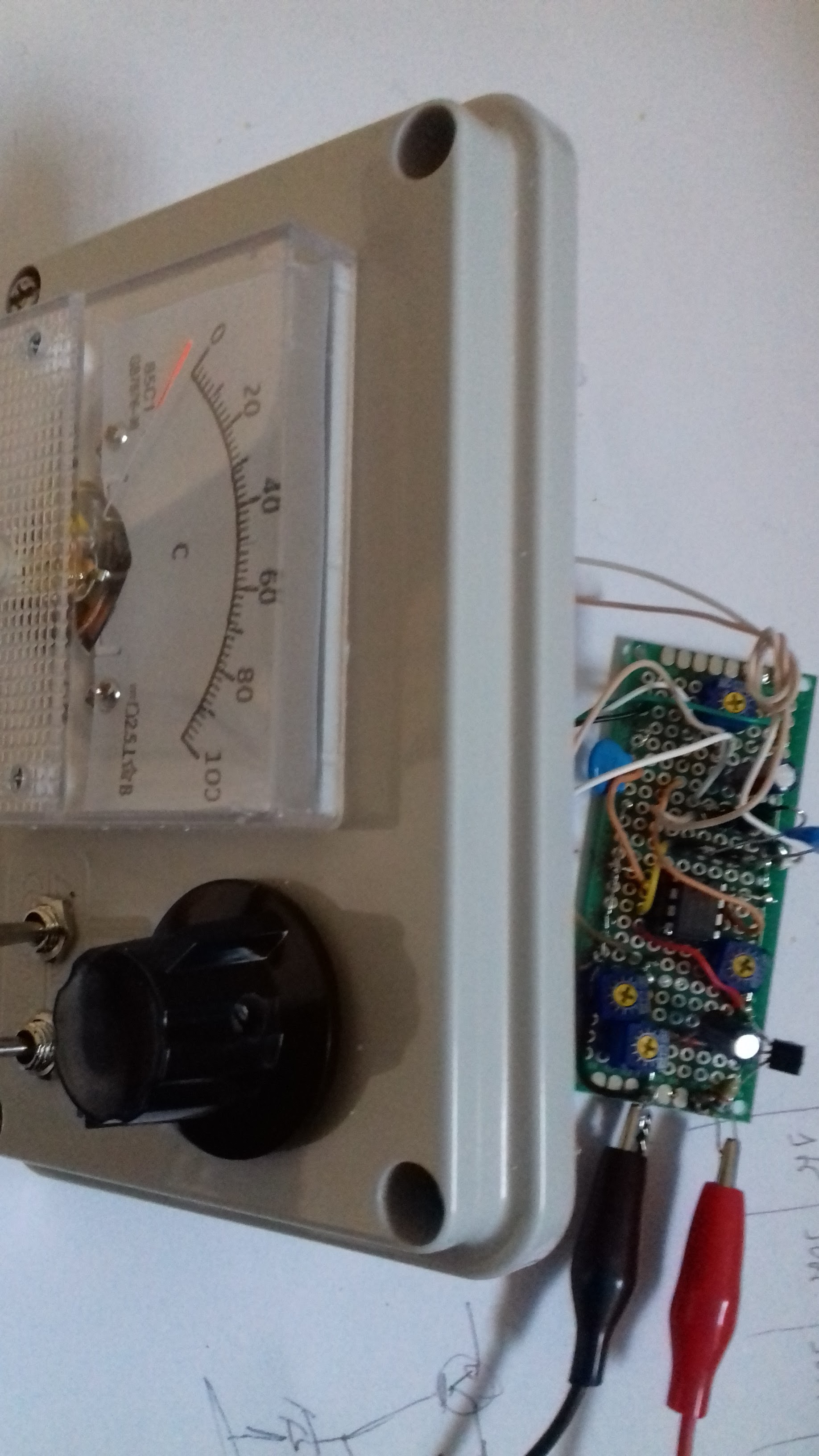
I won’t go into all of the details, but one of the checks he had made was to measure the continuity of the feed line, which is 80 feet of 18-gauge, 450 Ω ladder line. To do this, he connected the jumper wire in the photo at right across the ladder line in his shack and then measured the resistance at the antenna feed point.

The measurement that he came up with was 16 Ω. Well, the National Institute of Science and Technology (NIST) says that the resistance of 18-gauge solid wire should be about .0064 Ω/ft. Using that figure, the resistance should be somewhere near 1 Ω.

So, Paul asked me to bring over my DMM, which I did yesterday. We dropped the antenna, put my Fluke 79 across the feed point, and measured close to 16 Ω.

It didn’t make much sense, but the only reasonable explanation was that the problem with this measurement was the jumper wire. This was somewhat troubling to Paul, as he had a sentimental attachment to this jumper wire. It was given to him by a fellow who worked for him at Xerox, and he pointed out to me how well-made it was. He noted, for example, that each end of the wire had been tinned before it was screwed to the alligator clip.

I agreed that it was well-made, but certainly one or both of the connections could have oxidized, resulting in a high-resistance connection. And guess what? When I measured the resistance of the jumper, it turned out to be about 15 Ω!

I then unscrewed the wire at one end and measured again. It measured 15 Ω. I unscrewed the wire at the other end, and voilá, I measured 0 Ω. I screwed the alligator clips back on, and the overall resistance was near 0 Ω again. My guess is that the second connection was a little loose, and that over the years, some oxidation built up on both the wire and the alligator clip.

Whenever we do something like this, Paul likes to ask, “So, what did we learn from this?” In this case, I think what we learned is that even jumper wires can go bad. It’s also a validation of the KB6NU Theory of Electronic Failures, i.e. at least 80% of the problems associated with electronic equipment are problems with cables or connectors.


Conversion of NOELEC style balun board to 1:1 – through measurement

By: Owen
3 May 2024 at 09:52

Conversion of NOELEC style balun board to 1:1 left readers with a challenge to measure the through performance of the modified balun board.

The link grounding the centre tap was cut for this test to float the secondary so that one side could be grounded. This will give almost identical response to the case where the centre was grounded.

Above is the test configuration, the yellow thing is a top view of a modified plastic clothes peg which is used to clamp one of the wires from the transformer to the SMA threads.

Above is a close up view of the connection without the clothes peg in place, there would not be as much as 3mm of conductor between the grey block and the SMA connector. The wire is 0.5mm diameter single core copper stripped from LAN cable.

Test jigs do not need to be expensive to be effective.

Above, a view of the modified clothes peg from another article.

Above is a plot of |s21| to 150MHz. The compensation causes a self resonance at about 180MHz, so whilst improving its InsertionVSWR at lower frequencies, it limits its useful range to about 150MHz.

This plot would commonly be labelled a “loss” plot by hammy Sammy… you know, the guy who says the attenuation or loss in my coax is -2dB/100′.

So, to be clear, it is as labelled the magnitude of s21 expressed in dB and that is equivalent to InsertionLoss. See Measurement of various loss quantities with a VNA for further explanation.

So what is really interesting is to drill down on InsertionLoss.

Above is a plot of InsertionLoss and its components (Transmission) Loss and MismatchLoss.

(Transmission) Loss is due mainly to core loss and to a lesser extent some wire loss, and it results in conversion of electrical energy to heat.

Note that MismatchLoss is very low mid-band, and becomes greater at the lowest frequencies and at the high end. The low end is degraded by high magnetising admittance (too few turns for the frequency, core type). Again, compensation whilst improving the mid band does so at the expense of degrading high end performance. Nevertheless, the module is quite good for many purposes from 400kHz to 150MHz.

Last update: 6th May, 2024, 6:42 AM

Conversion of NOELEC style balun board to 1:1

By: Owen
1 May 2024 at 23:00

This article describes a small 1:1 balun for use in measuring field strength using a TinySA Ultra and a small loop antenna.

The balun is also useful for measurements using the NanoVNA (or any VNA), eg for measuring two wire transmission line parameters.

Materials

Some “TC1-1T RF Balun Transformer 0.4-500MHz 1:1CT” transformers were purchased on Aliexpress, 5 for $7. The part number is a Mini-circuits part, but these are likely to be clones. The balun boards also came from Aliexpress, about $4 each. Also needed are compensation caps of 10pF (0805).

Conversion

The boards come with a nominal 1:9 transformer and in my experience a capacitor (though I think the NOELEC board may use a TVS). In any event, it should be removed and the transformer removed. Fit the new transformer and solder a short circuit across the cap pads.

High end compensation

See High end VSWR compensation in a ferrite cored RF transformer for an explanation of compensation.

Connect the board to VNA Port 1 and sweep it to 200MHz, adjusting s11 e-delay so that the trace is a dot at the left of the Smith chart X=0 line. This adjusts the reference plane approximately to the position of the capacitor. Write down the e-delay value for later.

Above is the modified transformer and some calibration parts loads. There are two loads, 200Ω 1% and the other has 2×100Ω 1% in parallel to give 50Ω 1%. The calibration parts are made on ordinary long header pin strips, break three off and pull the middle one out with pliers. Slide the pins to a suitable projection and cut off the other end to uniform length then solder the resistors or shorts to them. This calibration effectively sets the Port 1 coupler Directivity to 46dB (which is quite good).

Measurement

So now, remove the short circuit on the cap pads and fit an accurate 50Ω load to the output terminals (such as the one pictured) and sweep 1-200MHz saving the .s1p file.

Open Simsmith and create a new model specifying the .s1p file for element L. Set the sweep to use L.FILE and you should get a L SWR trace like the magenta one above.

Now insert a compensation capacitor (C1 above) and set it to 10pF. Display G SWR and it should be like the blue trace above. Adjust C1 for best compensation to find your optimal compensation capacitor.

Now fit the capacitor, and sweep the balun again to confirm that it now has a response like the blue trace above.

Above is a sweep from 0.1-2.1MHz, the transformer should be usable down to 400kHz.

Above is a sweep from 1-201MHz. The limit of its useful range is determined by the application. It has quite good InsertionVSWR up to 30MHz, and good InsertionVSWR to about 150MHz.

More detail

Adjust the s11 e-delay to 250ps less than the figure you wrote down earlier, this moves the reference plane to approximately the far of the SMA connector so that R and X values are meaningful.

Above is the InsertionVSWR plot from 0.1-201MHz displayed by overlaying the low frequency and high frequency sweeps in NanoVNA-App.

Above is a ReturnLoss view of the same data.

Above is R,X of the same data. Note the effect of compensation is to turn X downwards as the frequency increases.

Above is the Smith chart view.

Grounded centre tap

There is a jumper on the back of the board which grounds the secondary centre tap. You may want to cut it for some applications. My own experience in measuring samples of two wire line is that it is better grounded. If you cut it with a fine cut, the connection can easily be remade with a dot of solder.

Other transformers

Other transformers can be used, though compensation depends on the transformer leakage reactance to a large degree.

Off the shelf 1:4 transformers are readily available, and work well though with a larger compensation cap.

You could wind your own transformer on a very small ferrite core. The smaller the core, the easier to obtain good broadband performance.

An exercise for the reader

Measure your own including s21. To measure s21, cut the ground link under the board for the centre tap so that the secondary is isolated and you can connect it to Port 2 with very short wires. It is not exactly the same, but it is a very good approximation.

Last update: 11th May, 2024, 4:29 AM

Simple ESR meter

 Almost a copy from here.


Only added provision for self "TEST", that is; the switch disconnects the terminals and connect internally to know resistor values via rotary switch (minimum 2 Ohm since had nothing smaller at the time). Also add zeroing via a pot on R24 place.

Diagram from the original site:


Inside:


and during testing:

Works nice, handy for testing old caps.

Have a nice day!


Simple Capacitance Meter

 As title says; a simple capacitance meter.

One youtube video by VK3YE was enough to get me started building, after all, the meter that I was using before was not behaving correctly (latter found the problem).

The outcome was this:

(scale on the left switch is wrongly printed, where is x2 should be x0.5/divide by 2)

During build:

Making the scale:
The scale on the meter was changed from the original 0-50 to 0-100, the easiest way was to scan the original face-place and then edit on a image editor.

To calibrate I used a 68pF and 27pF capacitor, the idea was not to have highest precision possible only to be in a position of having certain about unmarked capacitors.

Some description/schematic from here and here:

I used different Ge diodes and the 10K pot was changed for 2 of 5K in series to give better adjustment range. The Zener was changed to 6.8v.
Ranges like this:

E: 100pF
D: 1nF
C: 10nF
B: 100nF
A: 1uF


Have a nice day!


10Ghz downconverter for 1.5Ghz spectrum Analyser

Had this build for some time, now it's time to show. 


 I was doing some experiments on the 10Ghz band and wanted a way of looking at the signals. Because the spectrum analyser I have only good to 1.5Ghz had to find a cheap way of doing it to get this:


Here looking at the third harmonic from an ADF4351 on 3.3Ghz after a pipe cap 10Ghz filter experiment.
 

The diagram explanation: a dbm mixer (Watkins-Johnson M80LCA) with a local oscillator based on a FVC99 10Ghz oscillator module (cheapest VCO I could find for 10Ghz). Some preamps on the input and output using 2Ghz preamp modules and replacing the MMIC amplifiers for the ones like Corvo NLB300 or ERA-1 that are good to 10Ghz.


The basic design:


 To this diagram I added a 6db directional coupler inline with the FVC99 VCO (used a Omni Spectra PN2023, good from 8 12.4Ghz) so I could measure the LO frequency and PLL it.

There is no stability control on the FVC99 oscillator, still working on a PLL system (maybe one of these days) but in my case I have two select positions, one: VCO is controlled by a single pot (like on the diagram) and the other position controlled by an EIP371 frequency counter (from the Lo Out via directional coupler) that makes the PLL loop. With EIP371 and since the output voltage of the loop is very small the control range seats near 9.5Ghz, there is an option of extending the range like on the EIP manual:

Or with a similar diagram, a multiply by 10 of the PLL voltage out of the EIP371, that would be enough to use the full range of the FVC99.

For now I use 9.5 Ghz if using the EIP371 for more stability and around 10Ghz set by the pot ("Flo" on the panel) if it's just a quick test.

Here the EIP working as external PLL controling the FVC99 so the LO gets more stable.


On the Rigol DSA815 spectrum analyser you can set the input offset to get the display right on the band of interest

Displaying here a 10Ghz signal using the 9.5Ghz Lo frequency

If you want to just check if the signal is around there, no need to use external PLL control to the FVC99, the "stability" with a simple potentiomenter  is enough.

Inside view:

The VCO adjust pot (top right in blue) is glued directly to the front panel

Some other images during prototype development:


Here one of the firsts tests, just an input amplifier, the mixer, the VCO and VCO amplifier and the mixer IF output directly to the spectrum analyser.

Testing during early days of the prototype with a 10Ghz homemade flange to SMA adapter and a pipe cap filter:


Anyhow, not a measuring device but it serves the purpose of checking if you have any signal around the 10Ghz band and for experiments, still very happy with the outcome and sensitivity.


Have a nice day!


ADF4351 signal generator with sweep

Nothing major here, needed a small signal generator to test in the 10Ghz range (using harmonics from 3.3Ghz), decided to go with the ADF4351 module available everywhere. This is an improvement over the previous iteration here.
After the initial testing on 3.3Ghz made some changes on the software in order to set some common frequencies for future testing with QO-100 satellite equipment and also added provision to sweep around the frequency currently set in order to test some filters. Output on 3.4Ghz:
And testing the third harmonic:
The Rigol is not a 10Ghz version, I'm using a down converter before the input, that will be another post... The diagram, at this stage I still didn't added the two extra buttons (look on code for mode and band), to change band and to change mode between set frequency and sweep.
Inside on the almost final interaction (waiting SMA's to connect to front pannel):
And the front panel view working:

The code on the current version, keep in mind might still have some bugs, reach me for latest version if there is one: If blogger breaks formatting ask me a copy by email. 

/*!
   ADF4351 signal generator
   
   CT2GQV 2020
   v1.4

   Based on code from: ADF4351 example program https://github.com/dfannin/adf4351

   VFO with 100Khz steps starting from a predifined frquency (UL frequencia) using 2 buttons for up and down.
   Display on 16x2 I2C LCD of the frequency set and the third harmonic value
   Also serial output of the main frequency set.
   Possibility to sweep for filter testing.
*/

#include <Arduino.h>
#include "adf4351.h"
#include <LiquidCrystal_I2C.h>

#define SWVERSION "1.4" // 2021-09-11
#define PIN_SS 9  ///< SPI slave select pin, default value
ADF4351  vfo(PIN_SS, SPI_MODE0, 1000000UL , MSBFIRST) ;
                       
//unsigned long frequencia = 3333320000UL ; // 3.333.334 (10 Ghz n=3)
unsigned long frequencia = 3496500000UL ; // 3.496.000 (10.489 Ghz n=3)
unsigned long maxfrequencia;
unsigned long minfrequencia;

// unsigned long frequencia = 2000000000UL ; // 2.000.000 (10 Ghz n=5)
// unsigned long frequencia =    414000000UL ; //    414.000 (10.368 Ghz n=25)
// for 442Mhz use the bellow and comment the above
//   unsigned long frequencia =  442000000UL ; // 442Mhz or 1.326 Ghz , tird harmonic

// I2C LCD virtual pinout
#define I2C_ADDR    0x27  // I2C Address for my LCD, found with I2C scanner
#define BACKLIGHT_PIN     3
#define En_pin  2
#define Rw_pin  1
#define Rs_pin  0
#define D4_pin  4
#define D5_pin  5
#define D6_pin  6
#define D7_pin  7
LiquidCrystal_I2C       lcd(I2C_ADDR, En_pin, Rw_pin, Rs_pin, D4_pin, D5_pin, D6_pin, D7_pin);

// buttons for up/down in frequency, puleed up from 5v with a 10K resistor, analog pin will be short to ground for button press

int button0 = 0; // mode
int button1 = 1; // up
int button2 = 2; // down
int button3 = 3; // select / band / step

int opmode = 0; //
int tempopmode = 0; //
int band = 0;
// Band 0 - 10Ghz (3.3Ghz harmonic) - 10489.550 to 10489.795MHz ->
// Band 1 - 2400.050 frequencia = 2400500000UL
// Band 2 - 1969.5Mhz (-2400 = 431Mhz )
// Band 3 - 2256 (2400-144Mhz) - 2400.050 to 2400.295MHz
// band 4 - 739.55 - LNB out

void setup()
{
  Serial.begin(9600) ;
  Serial.print("adf4351 VFO CT2GQV "); Serial.println(SWVERSION) ;

  pinMode(button0, INPUT); // mode
  pinMode(button1, INPUT); // up
  pinMode(button2, INPUT); // down
  pinMode(button3, INPUT); // band

  lcd.begin (16, 2, LCD_5x8DOTS); lcd.setBacklightPin(BACKLIGHT_PIN, POSITIVE); lcd.setBacklight(HIGH); // 20x4 lines display LCD
  lcd.home();
  lcd.setCursor(0, 0);  lcd.print("Signal Generator  ");
  lcd.setCursor(0, 1);  lcd.print("Ver: "); lcd.print(SWVERSION);

  Wire.begin() ;
  /*!
     setup the chip (for a 10 mhz ref freq)
     most of these are defaults
  */
  vfo.pwrlevel = 3 ; // measured at 3.3Ghz after 1m cable >> "0" = -8 dBm / "1" =  -5.8dbm / "2" = -3.3dbm / "3" = -0.4dbm
  vfo.RD2refdouble = 0 ; ///< ref doubler off
  vfo.RD1Rdiv2 = 0 ;   ///< ref divider off
  vfo.ClkDiv = 150 ;
  vfo.BandSelClock = 80 ;
  vfo.RCounter = 1 ;  ///< R counter to 1 (no division)
  vfo.ChanStep = steps[2] ;  ///< set to 10 kHz steps

  /*!
     sets the reference frequency to 10 Mhz
  */
  if ( vfo.setrf(10000000UL) ==  0 )
    Serial.println("REF.SET: 10 Mhz") ;
  else
    Serial.println("ERROR: reference freq set error") ;
  /*!
     initialize the chip
  */
  vfo.init() ;

  /*!
     enable frequency output
  */
  vfo.enable() ;

  delay(500);
  lcd.clear();

  if ( vfo.setf(frequencia) == 0 ) {
    Serial.print("VFO.SET:") ; Serial.println(vfo.cfreq) ;
    lcd.setCursor(0, 0);  lcd.print("F   :"); lcd.print(frequencia/1000);
    lcd.setCursor(0, 1);  lcd.print("F(3):"); lcd.print((frequencia/1000)*3);
  } else {
    Serial.println("ERROR: Set init Frequency") ;
  }

vfo.ChanStep = steps[4] ; ///< change to 100 kHz
}

void loop()
{
  int buttonState0 = analogRead(button0); // mode
  int buttonState3 = analogRead(button3); // band
 
  int buttonState1 = analogRead(button1); // up
  int buttonState2 = analogRead(button2); // down
  // serial debug for the button for +/- frequency
  // Serial.print("B1,B2:"); Serial.print(buttonState1); Serial.print(",");  Serial.println(buttonState2);


// band / start/stop sweep
  // button pin is puled down to ground...or close to it (100) as long as lower than 2049
  if (buttonState3 <= 100) {
    {


   if (opmode == 1 ){  
       /////// start stop start procedure
       if(tempopmode == 1) // started
        {
        lcd.clear();
        lcd.setCursor(0, 0);  lcd.print("SWEEPING starded ");
        lcd.setCursor(0, 1);  lcd.print("Stop---------->  ");   
        tempopmode = 255;
        maxfrequencia=frequencia+10000000; //compute the max frequency so we start from the one now and 100Mhz down and up
        minfrequencia=frequencia-10000000; //compute the min frequency so we start from the one now and 100Mhz down and up
        delay(150);
        }
        else // is stoped
        {
        lcd.clear();
        lcd.setCursor(0, 0);  lcd.print("SWEEPING stoped ");
        lcd.setCursor(0, 1);  lcd.print("Start---------->");
        tempopmode = 1;
        delay(150);
       }
   };
      
    // we are in band mode
    if (opmode == 0 ){            
      Serial.print ("BAND: ");
      band++;
      if (band > 4){band=0;};
      if(band == 0){
        frequencia=3496500000UL;
        vfo.setf(frequencia);
        lcd.clear();
        lcd.setCursor(0, 0);  lcd.print("F   :"); lcd.print(frequencia/1000);
        lcd.setCursor(0, 1);  lcd.print("F(3):"); lcd.print((frequencia/1000)*3);  };
      
      if(band == 1){
        frequencia=2400500000UL;
        vfo.setf(frequencia);
        lcd.clear();
        lcd.setCursor(0, 0);  lcd.print("F   :"); lcd.print(frequencia/1000);
        lcd.setCursor(0, 1);  lcd.print("TX QO100         ");   };
      
      if(band == 2){
        frequencia=1969500000UL;
        vfo.setf(frequencia);
        lcd.clear();
        lcd.setCursor(0, 0);  lcd.print("F   :"); lcd.print(frequencia/1000);
        lcd.setCursor(0, 1);  lcd.print("+430Mhz QO100 TX");  };
      
      if(band == 3){
        frequencia=2256000000UL;
        vfo.setf(frequencia);
        lcd.clear();
        lcd.setCursor(0, 0);  lcd.print("F   :"); lcd.print(frequencia/1000);
        lcd.setCursor(0, 1);  lcd.print("+144Mhz QO100 TX");  };

      if(band == 4){
        frequencia=739550000UL;
        vfo.setf(frequencia);
        lcd.clear();
        lcd.setCursor(0, 0);  lcd.print("F   :"); lcd.print(frequencia/1000);
        lcd.setCursor(0, 1);  lcd.print("LNB OUT 10.48955");  };

        Serial.println(band) ;
      
     }; // let's change band
               
    };
  }
// end band up  

// mode  
  if (buttonState0 <= 100) {
    {
      if(opmode == 0)
      {
        opmode=1; tempopmode = 1;
        Serial.print ("SWEEP MODE:"); Serial.print(opmode);  Serial.print(","); Serial.println(tempopmode) ;
        lcd.clear();
        lcd.setCursor(0, 0);  lcd.print("SWEEPING MODE   ");
        lcd.setCursor(0, 1);  lcd.print("START/STOP----->");   
        delay(150);       
      }
      else
      {
        opmode=0; tempopmode =0;
        Serial.print ("BAND MODE:"); Serial.print(opmode);  Serial.print(","); Serial.println(tempopmode) ;
        lcd.clear();
        lcd.setCursor(0, 0);  lcd.print("F :"); lcd.print(frequencia/1000);
        lcd.setCursor(0, 1);  lcd.print("BAND MODE       "); lcd.print(frequencia/1000);
        
      };
      
    }
  } // end if (buttonState0 <= 100) {


// if we are sweeping
if (opmode==1 && tempopmode == 255){lcd.print(" .");};
if (opmode==1 && tempopmode == 255){lcd.print("  o");};
if (opmode==1 && tempopmode == 255){lcd.print("   O");};

if (opmode==1 && tempopmode == 255){
  frequencia += vfo.ChanStep; // increase frquency by step
  if (frequencia >= maxfrequencia){frequencia=minfrequencia;}; // if we are on the limit then go to lower value
  vfo.setf(frequencia);
   Serial.print ("F:"); Serial.println(frequencia) ;
 };


// up frequency
  // button pin is puled down to ground...or close to it (100) as long as lower than 2049
  if (buttonState1 <= 100) {
    frequencia += vfo.ChanStep;
    if ( vfo.setf(frequencia) == 0 )
    {
      Serial.print ("VFO.SET: "); Serial.println(vfo.cfreq) ;
      lcd.clear();
      lcd.setCursor(0, 0);  lcd.print("F   :"); lcd.print(frequencia/1000);
      if (band == 0 ){lcd.setCursor(0, 1);  lcd.print("F(3):"); lcd.print((frequencia/1000)*3);};
    }
  }
// end up frequency  

// down frequency
  if (buttonState2 <= 100) {
    frequencia -= vfo.ChanStep;
    if ( vfo.setf(frequencia) == 0 )
    {
      Serial.print ("VFO.SET: "); Serial.println(vfo.cfreq) ;
      lcd.clear();
      lcd.setCursor(0, 0);  lcd.print("F   :"); lcd.print(frequencia/1000);
      if (band == 0 ){lcd.setCursor(0, 1);  lcd.print("F(3):"); lcd.print((frequencia/1000)*3);};
    }
  }
// end down frequency  

 
 // button software debounce if we are not sweeping
 if (opmode == 0) {   delay(150); };
 
} // end code


 Have a great day!

ADF4351 Signal Generator

 Not much here, just a simple signal generator based on ADF4351 module from "fleebay". PS: there is an improvement over this code at this new post.


 I just needed to generate one single frequency that can go up or down in 100Khz steps via two push buttons. Added an optional LCD to display the main frequency and the third harmonic since I'm using it to verify some equipment on 10Ghz.

Test board:


On the frequency counter:


Schematic based on an Arduino Nano controler:

Spectrum output on lower frequencies (414Mhz) and output level at "0" (add 20db attenuation at the spectrum input):

and the third harmonic:

Power at "3" (second harmonic now visible)


 3rd harmonic as seen on a 10Ghz adapter for a 1.5Ghz spectrum analyzer:
(not calibrated):

Code:

 /// code start
/*!
   ADF4351 signal generator
  
   CT2GQV 2020
   v1.3

   Based on code from: ADF4351 example program https://github.com/dfannin/adf4351

   VFO with 100Khz steps starting from a predifined frquency (UL frequencia) using 2 buttons for up and down.
   Display on 16x2 I2C LCD of the frequency set and the third harmonic value
   Also serial output of the main frequency set.
*/

#include <Arduino.h>
#include "adf4351.h"
#include <LiquidCrystal_I2C.h>

#define SWVERSION "1.3"
#define PIN_SS 9  ///< SPI slave select pin, default value
ADF4351  vfo(PIN_SS, SPI_MODE0, 1000000UL , MSBFIRST) ;
                      
unsigned long frequencia = 3333320000UL ; // 3.333.334 (10 Ghz n=3)
// unsigned long frequencia = 2000000000UL ; // 2.000.000 (10 Ghz n=5)
// unsigned long frequencia =    414000000UL ; //    414.000 (10.368 Ghz n=25)
// for 442Mhz use the bellow and comment the above
//   unsigned long frequencia =  442000000UL ; // 442Mhz or 1.326 Ghz , tird harmonic

// I2C LCD virtual pinout
#define I2C_ADDR    0x27  // I2C Address for my LCD, found with I2C scanner
#define BACKLIGHT_PIN     3
#define En_pin  2
#define Rw_pin  1
#define Rs_pin  0
#define D4_pin  4
#define D5_pin  5
#define D6_pin  6
#define D7_pin  7
LiquidCrystal_I2C       lcd(I2C_ADDR, En_pin, Rw_pin, Rs_pin, D4_pin, D5_pin, D6_pin, D7_pin);

// buttons for up/down in frequency, puleed up from 5v with a 10K resistor, analog pin will be short to ground for button press
int button1 = 1;
int button2 = 2;


void setup()
{
  Serial.begin(9600) ;
  Serial.print("adf4351 VFO CT2GQV "); Serial.println(SWVERSION) ;

  pinMode(button1, INPUT);
  pinMode(button2, INPUT);

  lcd.begin (16, 2, LCD_5x8DOTS); lcd.setBacklightPin(BACKLIGHT_PIN, POSITIVE); lcd.setBacklight(HIGH); // 20x4 lines display LCD
  lcd.home();
  lcd.setCursor(0, 0);  lcd.print("Signal Generator  ");
  lcd.setCursor(0, 1);  lcd.print("Ver: "); lcd.print(SWVERSION);

  Wire.begin() ;
  /*!
     setup the chip (for a 10 mhz ref freq)
     most of these are defaults
  */
  vfo.pwrlevel = 3 ; // measured at 3.3Ghz after 1m cable >> "0" = -8 dBm / "1" =  -5.8dbm / "2" = -3.3dbm / "3" = -0.4dbm
  vfo.RD2refdouble = 0 ; ///< ref doubler off
  vfo.RD1Rdiv2 = 0 ;   ///< ref divider off
  vfo.ClkDiv = 150 ;
  vfo.BandSelClock = 80 ;
  vfo.RCounter = 1 ;  ///< R counter to 1 (no division)
  vfo.ChanStep = steps[2] ;  ///< set to 10 kHz steps

  /*!
     sets the reference frequency to 10 Mhz
  */
  if ( vfo.setrf(10000000UL) ==  0 )
    Serial.println("REF.SET: 10 Mhz") ;
  else
    Serial.println("ERROR: reference freq set error") ;
  /*!
     initialize the chip
  */
  vfo.init() ;

  /*!
     enable frequency output
  */
  vfo.enable() ;

  delay(1000);
  lcd.clear();

  if ( vfo.setf(frequencia) == 0 ) {
    Serial.print("VFO.SET:") ; Serial.println(vfo.cfreq) ;
    lcd.setCursor(0, 0);  lcd.print("F   :"); lcd.print(frequencia/1000);
    lcd.setCursor(0, 1);  lcd.print("F(3):"); lcd.print((frequencia/1000)*3);
  } else {
    Serial.println("ERROR: Set init Frequency") ;
  }

vfo.ChanStep = steps[4] ; ///< change to 100 kHz
}

void loop()
{
  int buttonState1 = analogRead(button1);
  int buttonState2 = analogRead(button2);
  // serial debug for the button for +/- frequency
  // Serial.print("B1,B2:"); Serial.print(buttonState1); Serial.print(",");  Serial.println(buttonState2);

// up frequency
  // button pin is puled down to ground...or close to it (100) as long as lower than 2049
  if (buttonState1 <= 100) {
    frequencia += vfo.ChanStep;
    if ( vfo.setf(frequencia) == 0 )
    {
      Serial.print ("VFO.SET: "); Serial.println(vfo.cfreq) ;
      lcd.setCursor(0, 0);  lcd.print("F   :"); lcd.print(frequencia/1000);
      lcd.setCursor(0, 1);  lcd.print("F(3):"); lcd.print((frequencia/1000)*3);
    }
  }
// end up frequency 

// down frequency
  if (buttonState2 <= 100) {
    frequencia -= vfo.ChanStep;
    if ( vfo.setf(frequencia) == 0 )
    {
      Serial.print ("VFO.SET: "); Serial.println(vfo.cfreq) ;
      lcd.setCursor(0, 0);  lcd.print("F   :"); lcd.print(frequencia/1000);
      lcd.setCursor(0, 1);  lcd.print("F(3):"); lcd.print((frequencia/1000)*3);
    }
  }
// end down frequency 

 
// button software debounce
  delay(150);
}
/// code end

Some other signal generators based on similar modules and also the ADF4355:
http://f6kbf.free.fr/html/ADF4351%20and%20Arduino_Fr_Gb.htm
https://pa0rwe.nl/?page_id=1345 (for the ADF4355)


Have a nice day!

❌
❌