❌

Normal view

There are new articles available, click to refresh the page.
Yesterday β€” 9 October 2024owenduffy.net

Microsemi AN1819: A 700W Broadband Amplifier Using VRF2944

By: Owen
9 October 2024 at 16:17

Microsemi publishes an application note that includes design of a high power FET RF power amplifier: https://ww1.microchip.com/downloads/aemDocuments/documents/PSDS/ApplicationNotes/ApplicationNotes/1819_B.pdf.

This article calculates their design figures using Calculate initial load line of valve RF amplifier . Though the terminology in the calculator is oriented towards valves, it is applicable to designs using FET and BJT.

Above is the calculated solution. Some notes:

  • AN1819 ignores the device saturation voltage. The value use in the calculator is taken from the device datasheet at the expected current.
  • Vs is set to Vakmin+66V to reconcile with AN1819.
  • AN1819 ignores output network (transformer, band pass filters) loss, so network efficiency is set to 100% in the calculator to reconcile with AN1819, but it is unrealistically high… but they are selling FETs.

Calculated Rlaa (drain to drain in this case) is 12.45Ξ©, which reconciles with AN1819’s 12.5Ξ©. Note that the assumption that a practical transfomer of 1:2 turns ration would transform a 50Ξ© load to exactly 12.5Ξ© is naive, and of course there would be a bandpass filter in a practical transmitter.

Β 

Above is the load line plotted over the datasheet drain characteristic curves. As is often the case, the datasheet graph does not extend to VDS=69.5V, so the load line above is truncated.

Although drain efficiency is about 75%, in a practical transmitter, transformer losses and bandpass filter loss would result in efficiency closer to 65% (as can be see if a realistic network efficiency was entered into the calculator).

All that said, this is the beginnings of a practical design for a nominally 600W transmitter (perhaps less), or perhaps 1kW with a combiner for two such pallets.

I might note that nothing in AN1819 suggests that there is a valid Thevenin equivalent circuit for the PA as an RF source, much less that it is 50Ξ©.

Conclusions

Calculate initial load line of valve RF amplifier reconciles with AN1819.

AN1819 overestimates the power obtainable at the output of the transformer and necessary bandpass filter.

Last update: 10th October, 2024, 7:40 AM
Before yesterdayowenduffy.net

Eico 723 reverse engineering

By: Owen
7 October 2024 at 09:53

The Eico 723 was a 1961 tabletop A1 Morse transmitter with self contained ACpower supply and rated at 60W using 3x6DQ6-B valves.

In the day, transmitters were commonly rated for plate DC input power, probably as it was thought by regulator authorities that it was too challenging to measure RF power output reliably (and for the same reasons the license limitations were cast in DC input. This inflated the capability in terms of todays practice of specifying RF output power.

So, the manual states it has a 500V power supply and to tune / load for 120mA DC plate current.

The operation goes beyond the curves given in the valve datasheet… so a bit of extrapolation is needed to construct a design load line.

Above is a calculated solution making some assumptions about network efficiency.

Conclusion is that with good valves, and tuned / loaded as per the manual, this should make about 41W key down into a 50Ξ© load (though the output network is more flexible than that). The calculated 14W plate dissipation is within ratings (18W), so it is a conservative design from that point of view.

Above is the calculated load line laid over the plate characteristics plot.

I had a soft spot for 6DQ6-B when I was a kid at school. I was buying new ones for TV service (which funded my hobby) for $1.85 in the late ’60s, and I much preferred them over the war surplus 807s (which were cheaper at $0.50). Two up in a transmitter using TV power transformers driving a voltage doubling rectifier gave lots of HT which is the first step in getting good PA efficiency.

Whilst 6DQ6-B were apparently cheap back then, adjusted for inflation, that is equivalent to $28 in 2024. NOS sell for towards double that, so not so inexpensive now. Obtaining rated output with poor valves may be a challenge.

Last update: 7th October, 2024, 8:53 PM

EFHW compensation, or those little blue capacitors

By: Owen
7 October 2024 at 00:22

Constructors tend to copy popular designs, good or bad, and one of the components they see in pics online are the compensation capacitors connected across the 50Ξ© interface jack.

Single layer high voltage ceramic capacitors are popular, blue is the popular colour for high voltage ones, selected on specified capacitance and some very high voltage rating, often in the range of 3-6kV.

No, I didn’t forget Q, D, tan Ξ΄, or ESR… I left them out because constructors don’t seem to consider that part of the requirement.

So let’s review the sense of this.

Voltage rating

Q: What is the peak voltage in a 50 ohm load at 1kW?

A: 316Vpk.

So what is an appropriate capacitor rating with some safety margin?

1kV gives a 10dB safety margin at 1000W in 50Ξ©.

500V gives a 14dB safety margin at 100W in 50Ξ©.

So, you might ask why people seek out 6-20kV capacitors.

Q, D, tan Ξ΄, ESR

Q, D, tan Ξ΄, ESR are different metrics of the dielectric loss of the capacitor.

Let’s focus on Q. Q or quality factor is given by \(Q=\frac{|X|}{R}\). In admittance terms, we can also say \(Q=\frac{|B|}{G}\).

Power lost in the capacitor with a constant applied AC voltage can be calculated several ways, one is \(P=V^2 G=\frac{V^2 |B|}{Q}=\frac{V^2}{Q |X|}\)… the last can be convenient.

Another useful equation is \(P=\frac{V^2 2 \pi f C}{Q}\), so increasing voltage V, frequency f, and capacitance C increase dissipation; and increasing Q decreases dissipation.

So for example:

  • at 100W in 50Ξ©, V=70.7V;
  • if Ccomp was a 100pF 1kV capacitor and at 30MHzΒ  Q=100, |X|=53; and
  • P=0.943W.

1W dissipation will probably overheat a 8mm diameter disk ceramic capacitor, so whilst it easily withstands the applied voltage, it is not up to 100W continuous RF power.

For this scenario, Q needs to be perhaps 500 or more for capacitor temperature reasons.

RF capacitors

Capacitors are made with a wide range of dielectric chemistry, and within the broad ceramic capacitor category, dielectrics (and capacitors) are often denoted as Class 1 and Class 2. Class 1 dielectrics have much higher Q than Class 2, and Class 1 dielectric is often used for capacitors of 100pF or less, but Class 2 dielectric is used above that.

If you need say 120pF, it may be better to use two smaller capacitors in parallel as they are more likely to use Class 1 dielectric and you also get the benefit of a little more surface area to help with heat dissipation.

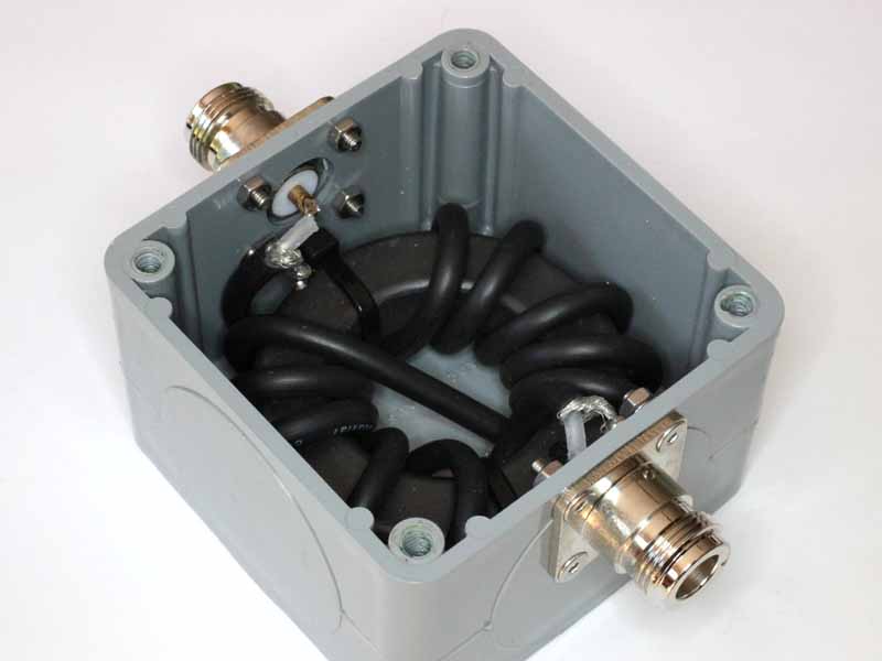
An example thermal analysis

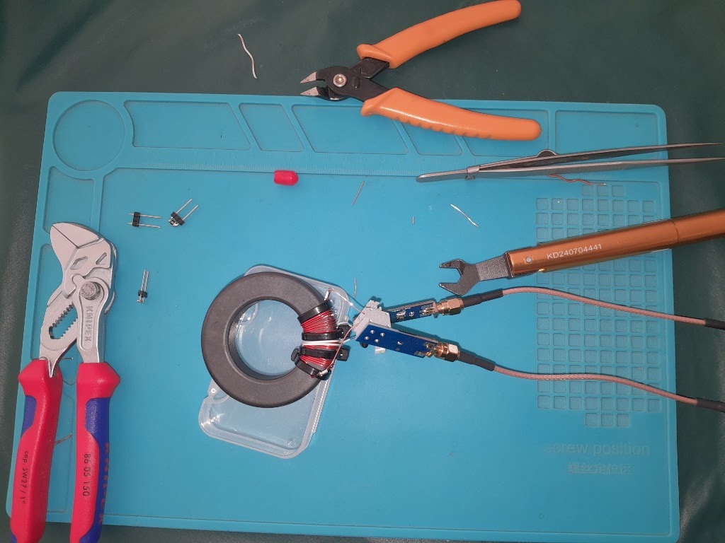
Above is the internals of a common mode choke which uses 10pF 3kV 6mm ceramic capacitors for compensation of the coax pigtails. Measured capacitor Q is 500 @ 30MHz.

Above is a thermal pic of the internals with temperature stabilised running 100W @ 30MHz. The capacitor temperature reaches 20.2Β°, a rise of 5.7Β° at estimated dissipation 18.5mW. Note that these small capacitors have very low specific heat capacity, the temperature stabilizes in just 10s in this example.

Note that the dissipation in a 100pF capacitor of the same Q would be 10 times as much, ~0.2W, and even though a 100pF capacitor has more surface area, it may overheat at that power (especially inside an enclosure with other heat sources).

You don’t need a thermal camera to evaluate your own build, if you cannot comfortably touch the capacitor at some power level, it is too hot and that is excessive power.

Transmission line stub

A transmission line stub may offer a practical alternative to a capacitor.

People often speak of one of the properties of a certain coaxial line as a certain capacitance per length, pF/m, and would suggest that since RG58A/U is specified as 101pF/m, then a length of 990mm would be equivalent to 100pF. That is quite naive.

Above is a plot of impedance components of 790mm @ 30MHz, and |X|=53, the same reactance as a 100pF capacitor, but somewhat shorter.

Above is a calculation from SimNEC of the power lost in the transmission line stub at 70.7V applied, the voltage due to 100W in 50Ξ©. Power lost is 0.7W which will result in a quite small increase in line temperature.

The example illustrates that such stubs are not equivalent to high Q capacitors, Q in this case is 130, not wonderful at all.

Let’s consider two shorter stubs in parallel.

Above is a calculation from SimNEC of the power lost in the transmission line stub at 70.7V applied, the voltage due to 100W in 50Ξ©. Power lost is 2*0.17=0.34W, half that of the previous case,Β which will result in a quite small increase in line temperature. Q in this case is 270, not wonderful, but better.

Now one advantage of the latter configuration is that it can be constructed by taking a single length of coax equal to the sum of the two stubs, forming into a shaped loop and connecting braid to braid and inner to inner at the ends to make a two terminal open circuit stub. There is no need to weatherproof the open ends that would otherwise exist.

Conclusions

For capacitors commonly used for compensation of RF transformers:

  • heating is an important limitation, and one that is commonly ignored;
  • extreme voltage rating is often uppermost in constructors minds, but that may be less a priority than thought, and may also lead to selection of a capacitor with poorer losses and higher operating temperature;
  • replacing a failed capacitor with a higher voltage rated one might not be the best solution;
  • transmission line stubs may provide a practical alternative; and
  • mindless copying of published designs might not produce good results.
Last update: 7th October, 2024, 6:26 PM

Toro MX4250 spindle maintenance

By: Owen
6 October 2024 at 00:51

The Toro MX4250 is a ZT ride on mower (riding mower).

I previously reported that after 200h, the original spindle bearings were in very poor condition, about 3mm of play at the blade ends, and they were replaced. There are lots of Chinese parts on this β€œmade in the US made” mower, so the bearings might well have been Chinese in origin.

The original spindles are not greaseable, and were fitted with 6203RS (rubber seals on both sides) ball bearings.

There is lots of stuff online about mower spindles, they are a significant maintenance problem.

A grab bag of online expert advice:

  • No need for greasing, the bearings are sealed for life (that might be less than 100h).
  • Modify residential spindles by adding a grease nipple like commercial mowers use.
  • RS bearings cannot be greased, the seal will pop out.
  • Punch the bearings out, remove the inner seals and put them back.
  • Fit a grease nipple and remove the rubber seal from the inside of both bearings.
  • Some commercial mowers are fitted with a grease nipple and metal shielded (ZZ) bearings.

Since these spindles hold a lot of grease, I intend greasing with a pneumatic greaser, and they tend to inject very quickly and the risk of an RS seal popping should be mitigated.

Above is a 6203ZZ (metal shielded) bearing. There is a gap of about 0.5+mm between bearing inner ring and the shield, shields are on both sides.

So, the path I have chosen to implement experimentally is to:

  • drill and tap the spindles and fit M6 grease nipples (make sure the grease nipple does not interfere with the internal spacers or shaft);
  • replace the bearings with 6203ZZ (metal shielded); and
  • grease the spindle at deck clean services (twice a year when blade type is changed, sharpened and balanced).

This work was done with the spindles fixed in the deck. The spindle bolts are renowned for seizing or shearing, and removal is probably best avoided.

The bearings can be punched out fairly easily, just display the spacer bush so that the punch can get purchase on the bearing inner. I always discard bearing that have had large force applied between inner and outer.

Above is a view of the spindle with grease nipple. The bearing at the blade end is recessed about 5mm into the housing, and the end of the shaft has a flange that fits into that recess, somewhat protecting the bearing from dirt and water.

Nevertheless, it would be imprudent to direct a high pressure washer directly at that area. That doesn’t prevent cleaning the outer area of the deck underside where grass accumulates.

Above is a view of the top of the spindle housing and the underside of the drive pulley. The bearing fits almost flush with the top of the housing, it would be imprudent to direct a high pressure washer directly at that area.

On this mower, the pully has a solid centre disc, no cutouts to make observing the greasing operation… but also no cutouts to let water jets into that area. An inspection mirror makes the job easy.

Time will tell whether the planned maintenance regime is practical and what bearing life is experienced.

What I chose to not do is simply buy a set of Chinese replacement spindles with grease nipples from eBay or Aliexpress… as I would still need to have replaced the bearings.

Now there are probably thousands of videos on this procedure on Youtube. If you are inclined to watch and learn, some key messages:

  • remove the pulley before removing the blade;
  • clean all swarf from inside the housing if you drilled and tapped for a grease nipple;
  • I never reuse a bearing that has been pressed out (or especially bashed out) by applying force between inner and outer rings (and that means use a tool like a suitable socket to drive the bearings in so you don’t apply force to the inner ring;
  • don’t forget to install the internal spacer if used… because if you find it later, you will need to knock a bearing out to install it (see above about reusing bearings damaged by removal);
  • this can usually be done without removing the spindle assembly from the deck, so avoiding the complication of corroded seized mounting bolts;
  • check the idlers as they wear out too;
  • before starting the engine, make sure the belt is free of obstructions and runs freely; and
  • grease it now and from time to time.
Last update: 9th October, 2024, 11:19 AM

Transformers and magnetic saturation

By: Owen
5 October 2024 at 06:26

It seems that even a basic but sound understanding of transformers challenges lots of hams, and even online experts that have been heard to brag of their qualifications so as to intimidate others who might question their words.

So at ARRL EFHW (hfkits.com) antenna kit transformer – revised design #1 – part 2 I estimated that at a current of 4Arms marked the onset of non-linear B-H response, ie the onset of saturation.

One online expert proposed a method that would rate this transformer at maximum 4^2*50=800W at which magnetic saturation would occur.

The referenced article estimated saturation at more like 17000W.

Some very basic transformer concepts

Let’s talk about some really basic transformer concepts.

The diagram above from Wikepedia shows a rectangular magnetic core with two windings, a primary and secondary on opposite limbs of the core.

Note the phase polarity markings (+ / -) and the direction of (conventional) alternating current.

An example for discussion

Above is an example power transformer for discussion,Β 240V 50Hz 100VA, n=Vs/Vp=1/20, rated primary current 0.416A, core mass around 800g, estimated core loss at 1W/kg is 0.8W, for a simple explanation, leakage is assumed zero and rated load is assumed purely resistive. Note that an AC power transformer is typically rated for primary voltage, frequency and VA, and that they are operated into the low end of BH saturation, a compromise between weight, dissipation and efficiency (and cost of course).

Let’s assume that it is a good design, and for a first analysis, let’s ignore flux leakage, ie flux due to current in one winding that does not induce voltage in the other winding (does not β€˜cut’ the other winding). Let’s analyse it with no load and rated load.

No load

With load load, assume zero current flows in the secondary.

The primary winding acts like an iron cored inductor, when voltage is applied, current flows. The current produces magnetic flux and a voltage induced in the primary winding which by Lenz’s law opposes the voltage that created the current.

The current that flows with no-load is known as the magnetising current, it establishes magnetic flux in the core.Β In a good design, the magnetising current is small wrt rated current. We can extend that and talk of the corresponding magnetising impedance and the magnetising admittance.

For the example 50Hz transformer shown, the magnitude of magnetising current is 12mA, 2.9% of rated current. Magnetising current is a component of primary current in a loaded transformer.

You might at first think that the magnetising impedance Zm is purely inductive, but that would make it lossless and nothing is lossless. In the example case, the phase of Zm is 74Β°, Zm=5556+j19213Ξ©.

Magnetising force is given by \(mmf=n(I_p +0.012 \angle -74°  – \frac{I_s}{n})=n 0.012 \angle -74Β° \text{At/m}\).

Rated load

So, when rated current flows in the secondary, it induces a voltage component in the primary winding that opposes the voltage induced in the primary by the magnetising current component, so more primary current flows… rated primary current in a zero leakage scenario.

Print the diagram and annotate it with a pencil, and work through Lenz’s law and the direction of current. Sure, I could have done it, but you will learn more by working through the solutions, you will remember it better, and get confidence in your growing analytical capability.

So, the primary current under rated load is the load current divided by the turns ratio, plus the magnetising current. In this example, Ip=0.416-0.012∠-74°.

Why does the core not saturate?

You need to calculate the net magnetising force by adding the primary and secondary magnetising force components. In this case, recalling that Is=Ip/n for our scenario, \(mmf=n(I_p +0.012 \angle -74°  – \frac{I_s}{n})=n 0.012 \angle -74Β° \text{At/m}\), the same as the no-load magnetising force.

Note that when leakage inductance and winding resistance are factored in, loaded magnetising force is usually a little less than no-load.

If load current does not cause saturation, what does?

Two common causes:

  • operating at lower that rated frequency; and
  • operating at higher than rated voltage.

Because the B-H response is non-linear, a small increase in primary voltage creates a disproportionate increase in core less (due to higher flux density).

But my guitar amp can be driven to transformer saturation!

Sure, it is being driven to higher voltage and or lower frequencies than the design point, both of which contribute to saturation. Changing the load impedance does not directly cause magnetic saturation.

My ferrite cored EFHW transformer is easily saturated!

Probably not. Naive users often incorrectly blame overheating of the ferrite core beyond the Curie point as magnetic saturation.

Conclusions

  • Lenz’s Law is key to understanding.
  • Increasing primary voltage or lowering frequency can cause magnetic saturation.
  • Increasing load current alone is unlikely to cause magnetic saturation.
  • Other non-linear behavior is often wrongly attributed to magnetic saturation.
Last update: 5th October, 2024, 5:04 PM

ARRL EFHW (hfkits.com) antenna kit transformer – revised design #1 – part 2

By: Owen
2 October 2024 at 21:37

This article continues on from several articles that discussed the ARRL EFHW kit transformer, apparently made by hfkits.com, and the revised design at ARRL EFHW (hfkits.com) antenna kit transformer – revised design #1 – part 1.

This article presents a saturation calculation.

You will not often see saturation calcs (for reasons that will become apparent), though you will hear uninformed discussion promoting FUD (fear, uncertainty and doubt).

Lets assume that the core is capable of maximum continuous power dissipation of 10W (limited by factors like safe enclosure temperature, human safety, Curie point etc).

Now let’s estimate the magnetising current for 10W of core dissipation with 3t primary

Starting with the expected permeability above…

Gm is the magnetising conductance, the real part of Y above, 0.00231.

We can approximate the primary voltage for 10W core dissipation as \(V=(\frac{P}{G_m})^{0.5}=(\frac{10}{0.00231})^{0.5}=65.8V\) which implies 87W in a 50Ξ© load.

Magnetising current can be calculated at 10W core dissipation as \(I_m=\frac{V}{|Z|}=\frac{65.8}{222}=0.296A\)

In fact, under load, the net magnetising force may be just a little below 0.296A due to the effects of leakage inductance.

Let’s estimate saturation current for a 3t primary

Lets assume that under load, magnetising force due to current in the secondary offsets most of the magnetising force due to current in the primary and that the net magnetising force is due to magnetising current.

So, let’s solve.

Above is Fair-rite’s published data for their #43 mix (do not assume it applies to pretenders). Let’s take saturation flux density to be 1500 gauss, 0.15T.

Above is a calc of the saturation current for the 3t primary (peak), 4.01 Arms.

Conclusions

The saturation current is 14 times the magnetising current at 10W core dissipation, and is unlikely to be a significant limitation for low duty cycle modes.

This EFHW transformer is loss limited rather than saturation limited for most practical applications.

If you had in mind that this transformer was suited to peak power \(14^2 \cdot 87=17000 \text{ W}\) or more, then it may be driven into saturation.

Last update: 4th October, 2024, 6:01 AM

Currents at a coax to dipole junction

By: Owen
30 September 2024 at 22:19

Ian White gives the following diagram to explain what goes on at the coax to dipole junction.

He labels five currents in his explanation.

Let’s simplify that

Above is a diagram from Common mode current and coaxial feed lines showing the currents where a coax connects two two wires.

Lets morph that to the dipole feedpoint topology.

The whole thing is defined by just two currents, I1 and I2. The common mode current Ic=I1-I2. There is common mode current present in the short two wire connection to the dipole, and on the outer surface of the coaxial cable.

Note that I1, I2 and Ic are usually standing waves (ie they vary with location), and so these currents are defined here at the point where the conductors meet the end of the coax.

Are the currents measurable?

Using a clamp on RF current probe, the currents on the each of the two dipole conductors I1 and I2 is measurable, and so also the current on the outside surface of the coax shield Ic.

Remember also that these are sinusoidal AC currents, and I1, I2 and Ic refer to the magnitude of the currents.

The three currents can be resolved into the common mode and differential components, see Resolve measurement of I1, I2 and I12 into Ic and Id
(I12=Ic, the current measured with the probe around both two wire conductors or around the outside of the coax.

Can the currents be measured at an elevated dipole feed point?

Sure. I have done measurements of Ic over the length of coax by hoisting a current probe on a separate halyard to raise and lower it and reading it from the ground with a spotting scope.

Recall that Ic is usually a standing wave, and when you measure it at just one point, you don’t know much about it.

Last update: 1st October, 2024, 1:46 PM

Fact check: β€œFor an antenna, if it doesn’t resonate, it really doesn’t radiate!”

By: Owen
30 September 2024 at 19:18

An example of the utter nonsense posted on social media.

My very first posting as a trainee was to Bringelly HF receiving station in 1970. It had Rhombic antennas every 30Β° of the compass, and a few other antennas, but the mainstay of operation was the set of Rhombics.

The nearby transmitting station at Doonside had a similar antenna arrangement of Rhombics fed with two or four wire open transmission lines to transmitters in a central building, for most operations, no coax involved between transmitters up to 30kW and antenna feed points.

Rhombics are an example of a non-resonant antenna, these were used for a large set of operating frequencies that were not harmonically related, were changed through the day with varying ionospheric conditions over the various circuits, within the broad frequency range of the Rhombics, and not restricted by a requirement for β€˜resonant length’ of radiator conductors.

You do not have to look hard for other examples of non-resonant length radiators that have good radiation efficiency.

Yet hammy Sammy thinks that β€˜resonance’, whatever it means, is a necessary condition for radiation efficiency.

In this case, the quote speaks to the credibility of the author.

Social media and errors

A further disadvantage of lots of social media platforms is the inability to edit mistakes. For example, one poster wrote in the same thread:

The qualitative conclusion here is that a β€œwild” impedance value of 890 – j418 which is far from resonance can and does yield an acceptable SWR.

My calc is that wrt 50Ξ©, that example has VSWR=21.7. We all make mistakes, but this appears locked in for perpetuity.

From the same thread:

The ONLY position on the (Smith) chart where resonance occurs is dead center or β€œbull’s eye”.

So, that depends on your meaning of resonance, and resonance of what? If you accept that X=0 is a requirement of resonance, then it is relevant that in the frame of reference being the Smith chart space, there is line from one side of the the Smith chart to the other where X=0, an infinite number of points ofΒ  β€˜resonance’.

And of course it is unsociable to call out factual error on social media.

Read widely, question everything.

So what happened to Bringelly and Doonside?

Bringelly part of the new western Sydney airport and Doonside is a major road interchange (the Light Horse Interchange).

Last update: 9th October, 2024, 10:27 AM

nanoVNA – are you fazed by phase?

By: Owen
25 September 2024 at 20:41

The NanoVNA can measure and display β€œphase”, is it useful for antenna optimisation?

Some authors pitch it as the magic metric, the thing they lacked with an ordinary SWR meter.

In a context where it seems most hams do not really have a sound understanding of complex numbers (and phase is one β€˜dimension’ of a complex quantity like voltage, current, S parameters, impedance, admittance etc), lets look at it from the outside without getting into complex values (as much as possible).

The modern NanoVNA can display three phase quantities, only two are applicable to one port measurements as would commonly be done on an antenna system:

  • s11 phase; and
  • s11 Z phase.

Let’s look at a sweep of a real antenna system from the connector that would attach to the transmitter (this is the reference plane), plotting the two phase quantities s11 phase and s11 Z phase, and SWR (VSWR) and a Smith chart presentation of the s11 measurement.

Above is the measurement of the antenna system.

Like most simple antenna systems (this is a dipole, feedline, ATU), the most appropriate optimisation target is SWR, and minimum SWR well above 7.1MHz.

The SWR is 2.568 at the desired frequency, it is poor.

Do either or both of the phase plots give useful information on the problem, and leads to fix it?

s11 phase

s11 phase is -179.62Β° at the desired frequency (the marker).

Some authors insist optimal s11 phase is zero, some with a little more (and only a little more) knowledgeable insist it should be either 0Β° or 180Β°, take your pick. In fact the latter criteria essentially means the load impedance is purely resistive… but let’s deal with that under the more direct measurement s11 phase of Z.

Phase of -179.62Β° is approximately -180Β°=180Β°.

This metric is not very useful in this case.

s11 phase of Z

s11 phase of Z is -0.4Β°, approximately zero, which means the load impedance is almost purely resistive.

Of itself, s11 phase of Z does not identify the shortcoming.

So, what is the shortcoming?

If SWR is the optimisation target as proposed for this type of antenna, the SWR is poor, and the minimum is at a significantly higher frequency.

The SWR plot is revealing.

For more information, the value of Z is reported for the Smith chart marker as 19.47-j0.140Ξ©.

The reason that SWR is not 1.0 is that the feed point impedance is not exactly 50+j0Ξ©, and the main reason is that the real component is quite low at 19.47 and less importantly there is some very small reactance.

So, this provides information that to improve the match, the real component needs to increase significantly, and some minor trimming of the imaginary component.

Let’s make some matching adjustments

The sweep above is after some adjustment seeking to optimise the match.

Overall, the SWR plot shows that SWR is now fairly good at 7.1MHz, the Smith chart shows the marker just left of the prime centre so R is a little low and X is close to zero, the marker detail shows that Z is 45.57-j0.426Ξ©, so a little more information than the SWR curve, and with more resolution than reading the Smith chart graphically, R is a little low, X is close to zero. This is good information to guide the next matching steps if one wanted to refine the match.

The phase plots are of almost no value.

Conclusions

  • Neither of the available s11 derived phase plots are of much use for this matching task.
  • The SWR plot gives the best high level indication of the match.
  • Knowledge of R and X components of Z can be helpful in understanding more detail of the match and guiding matching adjustments.
  • This article has not explained the Smith chart in detail, it requires an understanding of complex quantities, so outside the scope and prerequisite knowledge set out for this article. In fact the Smith chart provides insight well beyond any and all of the other plots.
Last update: 26th September, 2024, 8:35 AM

A low Insertion VSWR high Zcm Guanella 1:1 balun for HF – coax bend radius

By: Owen
19 September 2024 at 09:01

I see online discussion of specification bending radius for coax cables, and their application to ferrite cored common mode chokes.

A low Insertion VSWR high Zcm Guanella 1:1 balun for HF and follow on articles described a balun with focus on InsertionLoss.

Let’s remind ourselves of the internal layout of the uncompensated balun.

The coax is quality RG58A/U with solid polythene dielectric. The coax is wound with a bending radius of about 10mm, way less than Belden’s specified minimum bending radius of 50mm.

So, the question is does this cause significant centre conductor migration that will ruin the characteristic impedance:

  • when it was first constructed; and
  • through life.

Note the pigtails at each coax connector, they are a departure from Zo of the coax and the N type connectors. They can be seen as short sections of transmission line with Zo perhaps 200Ξ© or more. The effect of these is to transform impedance and so cause the input VSWR to depart from ideal.

When first constructed

Above is a chart from the original construction articles. InsertionVSWR @ 30MHz is about 1.15.

Note the pigtails at each coax connector, they are a departure from Zo of the coax and connectors. They can be seen as short sections of transmission line with Zo perhaps 200Ξ© or more. The effect of these is to transform impedance and so cause the input VSWR to depart from ideal.

After 5 years of service

This article presents measurement of the balun 5 years after it was made, 5 years in use, but not operated at temperatures above datasheet maximum.

As mentioned, the pigtails are the main contribution to InsertionVSWR. The balun was compensated using 10pF shunt capacitors at both coax connectors. (Possible compensation solutions were discussed at A low Insertion VSWR high Zcm Guanella 1:1 balun for HF – more detail #3).

Above is a NanoVNA screenshot of measurement of the compensated balun using the calibration LOAD, a couple of SMA(F)-N(M) adapters and a short SMA(M)-SMA(M) cable.

InsertionVSWR is highest at 1.01 @ 16MHz, at the limits of accuracy with this equipment. These 3kV 10pF ceramic capacitors have measured Q around 500 at 30MHz, expected loss is less than 200mW @ 1kW through.

The InsertionVSWR is not significantly affected by the quite small bending radius.

Voltage withstand

Does tight bending of this cable degrade voltage withstand of the balun?

Experience Hipot testing lots of baluns with this type of coax winding shows that the voltage withstand weakness is over the surface of the dielectric from braid to centre conductor, and pigtails of less than 15mm will flash over before internal flashover.

Alternative coax types

Coax with a solid PTFE dielectric is more suitable as the dielectric is harder and withstands higher temperatures before deformation.

Foamed dielectric cables are much more prone to migration of the centre conductor on tight bends, even at room temperature and are probably unsuitable for tight wraps.

Small diameter cables might seem the obvious answer, but they are higher in loss and will run at higher temperature.

Conclusions

Though the coax bend radius is substantially smaller than specification minimum bend radius:

  • when first constructed, there was little evidence that the coax characteristic impedance was altered by the winding radius, and that the pigtails were the main contribution to InsertionVSWR; and
  • after five years of service, the InsertionVSWR of the compensated balun is excellent, at the limits of accuracy of the test equipment and again, little evidence that the coax characteristic impedance was altered by the winding radius.

Solid dielectric coax may be quite satisfactory at static tight bend radius, subject to the temperature of operation and applied forces.

Last update: 30th September, 2024, 4:58 PM

Return Loss Bridge – Dunsmore’s bridge

By: Owen
17 September 2024 at 01:20

Jeff, K6JCA, kindly sent me a paper, (Dunsmore 1991) which gives design details for a variation of the common resistive Return Loss Bridge design.

This article expands on the discussion at Return Loss Bridge – some important details, exploringΒ Dunsmore’s design.

Dunsmore’s design

Above is Figure 3a from (Dunsmore 1991).

Exploration

The Dunsmore’s circuit has been rearranged to be similar to that used in my earlier articles.

Above is the rearranged schematic for discussion. It is similar to that used in the earlier article, but three components are renamed, R1, R2 and R3.

To analyse the circuit, we can use the mesh currents method. Mesh currents i1, i2 and i3 are annotated on the schematic.

The mesh equations are easy to write:

\(V_s=(zs+r1+r3) \cdot i1-r1 \cdot i2-r3 \cdot i3\\0=-r1 \cdot i1+(r1+r2+zd) \cdot i2-zd \cdot i3\\0=-r3 \cdot i1-zd \cdot i2+(r3+zd+zu) \cdot i3\\\)

This is a system of 3 linear simultaneous equations in three unknowns. In matrix notation:

\(\begin{vmatrix}i1\\i2\\i3 \end{vmatrix}=\begin{vmatrix}zs+r1+r3 & -r1 & -r3\\-r1 & r1+r2+zd & -zd\\-r3 & -zd & r3+zd+zu\end{vmatrix}^{-1} \times\begin{vmatrix}V_s\\0\\0\end{vmatrix}\\\)

Lets solve it in Python (since we are going to solve for some different input values) for Vs=1V.

First pass: zs, zref, zd are 50Ξ©, and zu is short circuit (1e-300 to avoid division by zero) for calibration and 25Ξ© for measurement.Β This example uses Dunmore’s 16dB coupling factor to derive the values for r1 and r3.

from scipy.optimize import minimize
import numpy as np
import cmath
import math

zs=50
zref=50
zd=50
c=0.5
c=10**(-16/20)
r3=zref/c-zref
r1=50
r2=zref**2/r3

print(c,r1,r2,r3)

#equations of mesh currents
#vs=(zs+r1+r3)β‹…i1βˆ’r1β‹…i2βˆ’r3β‹…i3
#0=βˆ’r1β‹…i1+(r1+r2+zd)β‹…i2βˆ’zdβ‹…i3
#0=βˆ’r3β‹…i1βˆ’zdβ‹…i2+(r3+zd+zu)β‹…i3

#s/c cal
zu=1e-300
#solve mesh equations
A=[[zs+r1+r3,-r1,-r3],[-r1,r1+r2+zd,-zd],[-r3,-zd,r3+zd+zu]]
b=[1,0,0]
#print(A)
#print(b)
res=np.linalg.inv(A).dot(b)
#print(res)
vcal=(res[1]-res[2])*zd
#print(vcal)

#check oc
zu=1e300
#solve mesh equations
A=[[zs+r1+r3,-r1,-r3],[-r1,r1+r2+zd,-zd],[-r3,-zd,r3+zd+zu]]
b=[1,0,0]
#print(A)
#print(b)
res=np.linalg.inv(A).dot(b)
#print(res)
vm=(res[1]-res[2])*zd
#print(vm)
rl=-20*math.log10(abs(vm)/abs(vcal))
print('ReturnLoss (dB) {:0.2f}'.format(rl))

#check 25
zu=25
#solve mesh equations
A=[[zs+r1+r3,-r1,-r3],[-r1,r1+r2+zd,-zd],[-r3,-zd,r3+zd+zu]]
b=[1,0,0]
#print(A)
#print(b)
res=np.linalg.inv(A).dot(b)
print(res)
vm=(res[1]-res[2])*zd
#print(vm)
rl=-20*math.log10(abs(vm)/abs(vcal))
print('Zu: {:.2f}, ReturnLoss: (dB) {:.2f}'.format(zu,rl))

This gives calculated rl=9.54dB which is correct. Also ReturnLoss for OC reconciles with the SC calibration.

This result is sensitive to the value of Zs and Zd, changing them alters the result. It may be that there are other combinations of Zs, Zd, r1, r2, r3 that give correct results in all cases.

A common manifestation of design failure is that ReturnLoss of a short circuit termination will be significantly different to an open circuit termination, and the difference may be frequency dependent when combined with imperfections in the bridge.

RF Directional Bridge: Operation versus Source and Detector Impedances

Jeff, K6JCA, published a very interesting articleΒ RF Directional Bridge: Operation versus Source and Detector Impedances that is relevant to the wider understanding of Return Loss Bridges.

Conclusions

Dunsmore gives an alternative design, though his formulas still depended on Zs=Zd=r1=Zref.

References

Dunsmore, J. Nov 1991. Simple SMT bridge circuit mimics ultra broadband coupler In RF Design, November 1991: 105-108.

Last update: 20th September, 2024, 7:33 AM

ARRL EFHW (hfkits.com) antenna kit transformer – revised design #1 – part 1

By: Owen
14 September 2024 at 20:57

This article continues on from several articles that discussed the ARRL EFHW kit transformer, apparently made by hfkits.com.

This article presents a redesign of the transformer to address many of the issues that give rise to poor performance, and bench measurement of the prototype. Keep in mind that the end objective is an antenna SYSTEM and this is but a component of the system, a first step in understanding the system, particularly losses.

This is simply an experimental prototype, it is not presented as an optimal design, but rather an indication of what might be achieved if one approaches the problem with an open mind instead of simply copying a popular design.

  • This prototype uses a Fair-rite 5943003801 core, equivalent in size to a FT240-43, it does not use NMG-H material (β€œAmidon 43”).
  • A 3t primary is used, barely sufficient but a substantial improvement on the original 2t primary.
  • The winding configuration is a primary of 3t and secondary of 21t, the secondary is close wound with 0.7mm ECW and the primary is wound using CAT5 cable wire wound over the middle of the secondary winding. This is done for two main reasons:
    • to permit some level of isolation of the β€˜radiator’ and β€˜counterpoise’ from the coax feed line with a view to reducing common mode current (most effective at the lower frequencies); and
    • to reduce leakage inductance with a view to improving broadband InsertionVSWR.

Leakage inductance

Leakage inductance is the enemy of broadband performance.

Total leakage inductance was assessed by measuring input impedance at 5MHz with the secondary shorted. Total leakage inductance is about 190nH (this slightly overestimatesΒ  leakage inductance due to resonance effects). This is two thirds that of the hfkits.com / ARRL original winding layout.

Through measurement with nominal load

The transformer is loaded with the nominal load comprising several 1% SMD resistors and VNA Port 2.

Β 

Above is a SimNEC design model, calibrated against measured input impedance with the nominal load.

Above is a pic of the measurement setup, a NanoVNA-H4 is to the right of the equipment shown. Note that the NanoVNA does not correct Port 2 mismatch error.

The transformers are described at Conversion of NOELEC style balun board to 1:1. The setup was SOLIT calibrated, the reference plane was the output side of the grey terminal blocks.

Above is a close up view of the prototype transformer with compensation capacitor. The loads are two 1% 2400Ξ© in parallel making 1200Ξ©, one in each secondary leg.

Measurement of the transformer was saved as a .s2p file.

Above is a SimNEC model importing the s2p file and adjusting for the voltage division of the 2400Ξ© and Port 2 impedance (assumed 50Ξ©, but uncorrected). The indicated Loss is just a little higher than predicted by the model, keep in mind that ferrites have quite wide tolerances.

Above is a plot of measured ReturnLoss and InsertionVSWR from the .s2p file.

Above is a plot of measured InsertionLoss from the .s2p file, and its components Loss and MismatchLoss.Β SeeΒ Measurement of various loss quantities with a VNA for discussion of loss terms.

Common mode impedance

Mention was made that the common mode impedance may help to reduce common mode current at lower frequencies. Zcm will look like a small capacitance below 10MHz, of the order of 10pF for the layout shown. For that reason, I would not deploy an inductive common mode choke near to the transformer, put it at the other end of the feed line.

Conclusions

This is simply an experimental prototype, it is not presented as an optimal design, but rather an indication of what might be achieved if one approaches the problem with an open mind instead of simply copying a popular design.

The revised transformer has substantially better performance than the original: ARRL EFHW (hfkits.com) antenna kit transformer – measurement .

The modifications are mainly about:

  • sufficient magnetising impedance; and
  • reducing leakage inductance.

Loss remains a little higher than I would, an opportunity for the reader to find further improvement, a learning opportunity!

Last update: 15th September, 2024, 11:30 AM

Jaycar L15 ferrite (LO1238)

By: Owen
9 September 2024 at 20:20

Jaycar’s LO1238 ferrite toroid is readily available in Australia at low cost and quite suits some HF RF projects.

The published data is near to useless, so a long time ago I measured some samples and created a table of complex permeability of the L15 material which I have used in many models over that time. It did concern me that measured Β΅i was about 25% higher than spec, which is the limit of stated tolerance. Keep in mind that this is Chinese product with scant data published.

I have measured some samples purchased recently, and Β΅i is closer to the specified 1000, so I intend using this new data in future projects.

Above is complex permeability calculated from s11 measurement of a single turn on the LO1238.

Downloads

L15.7z

Last update: 10th September, 2024, 6:20 AM

Probing the popular s21 series through impedance measurement using NanoVNA-D v1.2.29 cf NanoVNA-D v1.2.40

By: Owen
6 September 2024 at 23:34

Derivation of the expression for the unknown impedance in an s21 series through measurement arrives at the following expression:

\(Zu=(Zs+Zl)(\frac{1}{s_{21}}-1)\).

The diagram above is from (Agilent 2009) and illustrates the configuration of a series-through impedance measurement.

It is commonly assumed that Zs+Zl=100Ξ©, as is done in (Agilent 2001). That might be a reasonable assumption if the VNA correction scheme corrects source and load mismatch, but let’s consider the NanoVNA-H running NanoVNA-D v1.2.29 (Apr 2024) firmware (the current release).

It is good practice to validate a measurement system by measuring a known component. Let’s measure a 200Ξ© 1% resistor that measures 200.23Ξ© at DC (it is actually 2 x 0806 100Ξ© 1% resistors in series.

Above is the test setup, the SDR-kits test board fixture was SOLIT calibrated 1-31MHz using the parts shown at centre of the pic. The fixture is shown with a 200Ξ© 1% DUT that measures 200.23Ξ© at DC.

NanoVNA-H v3.3 with NanoVNA-D v1.2.29

Above is a screenshot from the NanoVNA-H measuring the SMD resistor that measures 200.23Ξ© at DC. The red and green traces use the internal feature to transform an S21 measurement into series thru impedance. The measured value of 204.9-j2.042Ξ© is significantly different to the expected 200.23Ξ©.

Above is a plot of calculated DUT assuming the Zs+Zl=100Ξ© (as does the screenshot above).Β  The measured values are significantly different to the expected 200.23Ξ©.

NanoVNA-D v1.2.29 does not correct source and load mismatch, and that is probably the main cause of the apparent error.

Lets turn the measurement around, if we measure some known impedance Zk, we can calculate Zs+Zl:

\(Zs+Zl=\frac{Zu}{(\frac{1}{s_{21}}-1)}\).

#import the network
nws21k=rf.Network(name+'-S21k.s2p')
zu=(50+50)*(1/nws21k.s[:,1,0]-1)
zk=200.23 #precision measurement of DUT resistor at DC
#calculate zs+zl using zu=(zs+zl)(1/s21-1) and zu=zk
zs_zl=zk/(1/nws21k.s[:,1,0]-1)

Above is a snippet of code in Jupyter to import the network and calculate the value of zs_zl (Zs+Zl) inferred by the s21 measurement of the DUT.

Above is a plotting of calculated zs_zl impedance components, real and imaginary, or R,X.

NanoVNA-H4 v4.3 with NanoVNA-D v1.2.40 using ERC

NanoVNA-D v1.2.40 (released 07/09/2024) includes optional Enhanced Response Correction which corrects source mismatch. The feature is turned on for these measurements.

The instrument was calibrated with a LOAD that measured 50.17Ξ© at DC, this was specified in the calibration.

The NanoVNA-H4 v4.3 has better Port 2 input impedance than the NanoVNA-H used in the previous tests.

All of these measures improve the accuracy of s21 series through measurement of Z.

Above is a screenshot from the NanoVNA-H4 measuring the SMD resistor that measures 200.23Ξ© at DC. The red and green traces use the internal feature to transform an S21 measurement into series thru impedance. The measured value of 199+j0.594Ξ© is different to the expected 200.23Ξ©, about 0.5%.

Above is a plot of calculated DUT assuming the Zs+Zl=100Ξ© (as does the screenshot above).Β  The measured values are significantly different to the expected 200.23Ξ©.

NanoVNA-D v1.2.40 does not correct load mismatch, and that is probably the main cause of the apparent error.

Lets turn the measurement around, if we measure some known impedance Zk, we can calculate Zs+Zl:

\(Zs+Zl=\frac{Zu}{(\frac{1}{s_{21}}-1)}\).

#import the network
nws21k=rf.Network(name+'-S21k.s2p')
zu=(50+50)*(1/nws21k.s[:,1,0]-1)
zk=200.23 #precision measurement of DUT resistor at DC
#calculate zs+zl using zu=(zs+zl)(1/s21-1) and zu=zk
zs_zl=zk/(1/nws21k.s[:,1,0]-1)

Above is a snippet of code in Jupyter to import the network and calculate the value of zs_zl (Zs+Zl) inferred by the s21 measurement of the DUT.

Above is a plotting of calculated zs_zl impedance components, real and imaginary, or R,X. Zs+Zl is considerably closer to ideal (100+j0Ξ©) than the previous case.

Conclusions

  • The analysis here is specific to a NanoVNA-H v3.3 running NanoVNA-D v1.2.29 and NanoVNA-H4 v4.3 running NanoVNA-D v1.2.40 configured as described.
  • The formula often given and implemented for transformation of a series through s21 measurement to impedance depends on an assumption that source and load ports have zero mismatch error (eg that any mismatch is corrected).
  • NanoVNA-D v1.2.29 does not correct source and load mismatch, the results are mediocre.
  • NanoVNA-D v1.2.40 combined with the improved NanoVNA-H4 v4.3 hardware does not correct load mismatch, but other improvements improve the accuracy.

References

  • Agilent. Feb 2009. Impedance Measurement 5989-9887EN.
  • Agilent. Jul 2001. Advanced impedance measurement capability of the RF I-V method compared to the network analysis method 5988-0728EN.
Last update: 7th September, 2024, 9:37 AM

Fox flasher MkII update 9/2024

By: Owen
5 September 2024 at 22:21

Fox Flasher MkII and several follow on articles described an animal deterrent based on a Chinese 8051 architecture microcontroller, the STC15F104E.

Fox flasher MkII update 7/2019 documented a rebuild of the enclosure etc.

This is an update after five more years operation outside.

Above is a pic of the device. The polycarbonate case has yellowed a little. Importantly the cheap PVA has not crazed, it is kept dry by the outer enclosure, and a hydrophobic vent helps keeps the interior dry.

The battery is a pouch LiPo single cell, it is in good condition. A previous trial with 18650 LiIon cells showed they were unsuitable for the environmentals.

Last update: 6th September, 2024, 8:21 AM

ARRL EFHW (hfkits.com) antenna kit transformer – measurement

By: Owen
5 September 2024 at 17:37

Two previous articles were desk studies of the the ARRL EFHW kit transformer, apparently made by hfkits.com:

This article documents a build and bench measurement of the component transformer’s performance, but keep in mind that the end objective is an antenna SYSTEM and this is but a component of the system, a first step in understanding the system, particularly losses.

The prototype

Albert, KK7XO, purchased one of these kits from ARRL about 2021, and not satisfied with its performance, set about making some bench measurement of the transformer component.

Above is Albert’s build of the transformer.

The kit parts list is as follows:

Magnetics

The first point to note is that Amidon’s 43 product of recent years has published characteristics that are a copy of National Magnetics Group H material (though they changed the letterhead).

Above is a side by side comparison of the NMG H material datasheet and Amidon 43, the Amidon appears to be a Photoshop treatment of the NMG.

Fair-rite have been a long term manufacturer of a material they designate 43 (which has changed over time), and it has been resold as such by many sellers. NMG H material is somewhat similar, but to imply it is equivalent to Fair-rite 43 might be a reach.

Overall design

I might note at the offset that the design is not original, there are countless articles on the net describing a 2:14 turn on a β€˜FT240-43’ transformer for an EFHW using exactly the same winding layout.Β  As discussed in other articles on this site, 2t is insufficient for operation down to 3.5MHz using Fair-rite #43, even worse for the National Magnetics H material published as Amidon 43.

Measurement

Measurements were made with a NanoVNA-H4. It is not a laboratory grade instrument, but well capable of qualifying this design and build.

Albert performed a two port measurement using the setup above. This places a nominal load on the transformer, and the voltage division of the series resistor and Port 2 input impedance is used to correct the measured s21 figure.

So let’s take the measurements and calibrate a SimNEC model of the transformer.

Above is the model using Fair-rite #43 material calibrated to measured leakage inductance and InsertionVSWR. The reconciliation of model (magenta) with measurement (green) is good. The equivalent Fair-rite part is 5943003801.

Let’s compare measurement to the same model but with Amidon 43 material (NMG-H):

Reconciliation is very poor at lower frequencies, the measured transformer appears to have significantly higher permeability.

Measure core complex permeability

Let’s take a diversion for a moment and put this question to bed.

Above is complex permeability calculated from measurement of a 1t winding on the core used above compared with the Fair-rite #43 2020 published data. Keep in mind that tolerances on ferrite are relatively wide, these two reconcile very very well, there is no doubt in my mind that the material is Fair-rite #43. This questions the seller’s specified parts list.

A similar plot against NMG-H shows a stark difference.

InsertionVSWR and ReturnLoss

So let’s return to the saved .s2p file from the two port measurement.

Above is a plot of bench measurement of ReturnLoss and (related) InsertionVSWR for the transformer with a nominal load.

The InsertionVSWR might look acceptable, but using InsertionVSWR as a single metric is a very limited view.

Above is a plot of InsertionLoss (-|s21|dB), and its components MismatchLoss and (Transmission) Loss. SeeΒ Measurement of various loss quantities with a VNAΒ for discussion of Loss terms.

Let’s dismiss performance below 7MHz, the plot shows it has insufficient turns.

Importantly, (Transmission) Loss is around 1dB at 7MHz, so 20% of the input power is converted to heat in the core and winding, mostly in the core. If you look back to the first SimNEC screenshot, the model predicts just under 1dB Loss, so measurement reconciles well with the prediction model.

Experience and measurement of Loss and thermographs informs that a transformer of this type in this type of enclosure is not capable of more than about 10W of continuous dissipation in typical deployments, less if it is in direct sun in a hot climate. That means the transformer is not likely to withstand more than about 50W average input power without damage or performance degradation.

Now that might be quite acceptable to some users, gauging by the number of web articles and Youtube videos recommending this, a lot of users apparently.

Credit

Credit to Albert for his interest in understanding these things, careful measurement of the prototype, and preparedness to dismantle the prototype for science.

Summary

So let’s end this article with the results of desk study and measurement:

  • though the kit specifications state the core is Amidon #43, the sample kit is almost certain to contain a Fair-rite 43 core which is significantly different;
  • two port measurement of the sample of one with nominal load showed around 1dB of Loss at 7MHz;
  • MismatchLoss grows rapidly as frequency is reduced below 7MHz suggesting it has insufficient magnetising impedance, a result of insufficient turns;
  • the winding configuration is not optimised for leakage inductance;
  • popularity is not a good indicator of performance.

Where to from here?

These problems beg a redesign and measure of the transformer… more to follow.

Last update: 7th September, 2024, 6:19 AM

DIY UHF short and open circuit terminations

By: Owen
4 September 2024 at 00:21

It is often handy to have a reliable / known female UHF short and open circuit terminations when measuring using cables terminated in a UHF male connector.

This article describes a DIY solution.

Above is a diagram from Rosenberger showing the location of the β€˜standard’ reference plane on UHF series connectors.

Above, the DIY short and open terminations. The short uses a M4x12 brass washer to short inner to outer at the connector body. This was measured using a VNA to have a one way propagation time of 50ps from the reference plane, and it is labelled for reference. The open termination simply has the pin cut off very close to the end of the dielectric, and again it measures 50ps.

These are not microwave standards, you are kidding yourself if you think you are making accurate measurements using UHF connectors above 100MHz, even less for demanding measurements.

You might wonder why you need an open termination. A UHF plug with a loose coupling sleeve and / orΒ  exposed male pin is not a reliable open with known location.

An example application is measurement of the above transformer (though with nominal load of 2450Ξ© attached by very short wires) using a short cable from the VNA to the UHF(F) jack, If the cable + SC adapter described above is calibrated with an e-delay value that shows X=0 over a wide range of frequencies,Β  removing the short termination and connecting the cable to the transformer (with load) allows capture of the impedance as exists at the point that the (blue) compensation capacitor is attached, ie we want the reference plane to be the inboard end of the UHF connector. In this case, we ignore the 50ps offset.

One could take that s11 data and apply a small +ve or -ve capacitance in shunt to evaluate whether the optimal capacitor is larger or smaller and by how much.

Above is an example of measurement a correspondent’s build of a hfkits.com EFHW transformer (aka ARRL EFHW transformer) imported to the L element as a .s1p file with reference plane at the UHF connector, and Ccomp is an additional +/- adjustment dialled up and down to optimise the VSWR response. In this case an additional 20pF provided a small improvement to VSWR on the higher bands.

For this technique to be valid, it is essential that the reference plane be where the compensation capacitor will be applied.

You wanted a LOAD as well? See A check load for antenna analysers with UHF series socket. If you want a UHF(F) load, do the same thing but with a UHF(F)-SMA(F) adapter.

Last update: 4th September, 2024, 10:46 AM

Probing the popular s21 series through impedance measurement using NanoVNA-D v1.2.29

By: Owen
2 September 2024 at 13:44

Derivation of the expression for the unknown impedance in an s21 series through measurement arrives at the following expression:

\(Zu=(Zs+Zl)(\frac{1}{s_{21}}-1)\).

The diagram above is from (Agilent 2009) and illustrates the configuration of a series-through impedance measurement.

It is commonly assumed that Zs+Zl=100Ξ©, as is done in (Agilent 2001). That might be a reasonable assumption if the VNA correction scheme corrects source and load mismatch, but let’s consider the NanoVNA-H running NanoVNA-D v1.2.29 (Apr 2024) firmware (the current release).

It is good practice to validate a measurement system by measuring a known component. Let’s measure a 200Ξ© 1% resistor that measures 200.23Ξ© at DC (it is actually 2 x 0806 100Ξ© 1% resistors in series.

Above is the test setup, the SDR-kits test board fixture was SOLIT calibrated 1-31MHz using the parts shown at centre of the pic. The fixture is shown with a 200Ξ© 1% DUT that measures 200.23Ξ© at DC.

Above is a screenshot from the NanoVNA-H measuring the SMD resistor that measures 200.23Ξ© at DC. The red and green traces use the internal feature to transform an S21 measurement into series thru impedance. The measured value of 204.9-j2.042Ξ© is significantly different to the expected 200.23Ξ©.

Above is a plot of calculated DUT assuming the Zs+Zl=100Ξ© (as does the screenshot above).Β  The measured values are significantly different to the expected 200.23Ξ©.

NanoVNA-D v1.2.29 does not correct source and load mismatch, and that is probably the main cause of the apparent error.

Lets turn the measurement around, if we measure some known impedance Zk, we can calculate Zs+Zl:

\(Zs+Zl=\frac{Zu}{(\frac{1}{s_{21}}-1)}\).

#import the network
nws21k=rf.Network(name+'-S21k.s2p')
zu=(50+50)*(1/nws21k.s[:,1,0]-1)
zk=200.23 #precision measurement of DUT resistor at DC
#calculate zs+zl using zu=(zs+zl)(1/s21-1) and zu=zk
zs_zl=zk/(1/nws21k.s[:,1,0]-1)

Above is a snippet of code in Jupyter to import the network and calculate the value of zs_zl (Zs+Zl) inferred by the s21 measurement of the DUT.

Above is a plotting of calculated zs_zl impedance components, real and imaginary, or R,X.

Conclusions

  • The analysis here is specific to a NanoVNA-H v3.3 running NanoVNA-D v1.2.29.
  • The formula often given and implemented for transformation of a series through s21 measurement to impedance depends on an assumption that source and load ports have zero mismatch error (eg that any mismatch is corrected).
  • NanoVNA-D v1.2.29 does not correct source and load mismatch.

References

  • Agilent. Feb 2009. Impedance Measurement 5989-9887EN.
  • Agilent. Jul 2001. Advanced impedance measurement capability of the RF I-V method compared to the network analysis method 5988-0728EN.
Last update: 3rd September, 2024, 10:00 AM

Jupyter: one for the toolbox – decompose common mode and differential mode current components

By: Owen
31 August 2024 at 04:58

This article is principally a short commendation for Jupyter or Interactive Python for ham radio related projects for the quantitative ham. Python is a cross platform programming language that has a very rich set of libraries to support scientific and engineering applications, and a good graph maker.

The exercise for this demonstration is to decompose three measurements of currents on a two wire transmission line at a point into the differential and common mode components at that point, and to plot a phasor diagram of a solution to the measurements. Remember that common mode current and differential current in an antenna system are usually standing waves.

Above is a diagram explaining the terms used, I1 and I2 are the magnitudes of currents in each conductor measured using a clamp on RF ammeter, and I12 is the magnitude of the current when both conductors are passed through the clamp on RF ammeter, i12 is the phasor sum of the underlying i1 and i2.

The solution to the problem lies in applying the Law of Cosines to find the angular relationship between the differential and common mode components, a high school trigonometry problem. In fact, we find the magnitude of the angle between ic and id.

Above is the solution, a phasor diagram taking id as the phase reference (ie 0Β°). Because we know only the magnitude of the angle between ic and id, there is a second possible solution as noted on the graphic.

Above is a screen capture of the Jupyter source cells and results.

When you look at the measurements that were taken, |i1| was within 2% of |i2| which many online experts would opine means there is nearly perfect balance. Measurement instruments based on simply comparing |i1| and |i2| indicating within the BalanceBarβ„’ are deeply flawed… though very popular.

The decomposition shows that the magnitude of the differential current |id| is 25.7A and the magnitude of the total common mode current is 9.3A (4.65A per leg). It is not nearly balanced!

This demonstration uses high school mathematics applied to three measurements of current to drill down on the distribution of currents in a scenario that many would regard as balanced. Balanced means that the currents in each wire are equal but opposite in phase at any point along the line.

A quotation from Lord Kelvin:

When you can measure what you are speaking about, and express it in numbers, you know something about it. But when you cannot measure it, when you cannot express it in numbers, your knowledge is of a meagre and unsatisfactory kind. It may be the beginning of knowledge but you have scarcely in your thoughts advanced to the state of science.

Last update: 1st September, 2024, 3:58 AM
❌
❌