Brad's Excellent VFO Story. Stable LC VFOs for Everyone --- Wisdom from the Masters
23 September 2024 at 02:07
![]()


Direct Conversion Receive System (Video Supplement)
I've built a lot of stages for this video -- but wanted to test a few of the better 50 Ω input Z audio preamps in an actual DC receiver. A functioning direct conversion receiver provides a good way to test for voltage and power amp instability & noises. I also wanted to get a feel for how much gain we really need despite all the mythos about this topic. With this supplement, I won't have to go into too much detail about the test receiver on the video.
My main receiver goal hasn't changed for 25 years — lift desired RF signals out of the ether with a decent signal to noise ratio while listening to a speaker at comfortable room loudness.
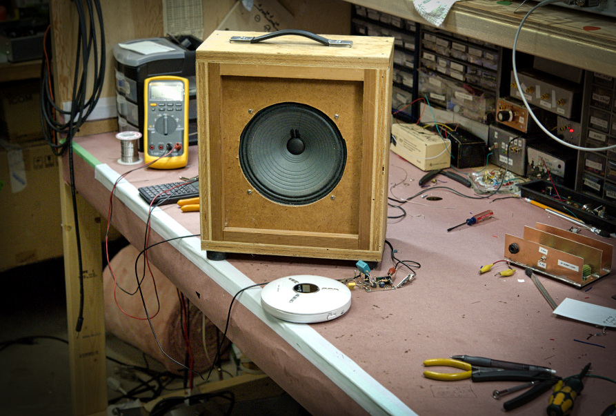
 Above — DC receive system. My chassis contains 2 BNC mixer input ports, an SBL-1 diode ring product detector, a post-product detector network and then 3 audio amplifiers plus a speaker jack. The AF amps = a 50 Ω impedance voltage amp, a second voltage amp with an active gain control - and finally a PA. I'll cover each AF stage separately, but first I'll show the complete receive system from inputs to output. Each stage lies on a separate piece of copper clad board. The active stages are numbered 1, 2 and 3. I soldered 2N4401 or 2N4403 for the BJTs.


Above — Schematic of the PA with DC measures. At this point, I did not add the 22 Ω DC decoupling resistor shown in the completed receiver. Few homebrew PA's will oscillate when tested stand-alone with a signal generator into a resistive load. I also took AC measures with my DSO.
A single voltage divider network feeds each of the 2 current sources. A 220 µF capacitor shunts voltage divider noise to ground.
My readers/audience asked me to make a single DC supply audio PA only using TO-92 transistors as finals.This is it. I worked hard to find a solution where the maximum output transfer function would compare with the venerable LM386 -- and bonus -- this final transistor pair tend to not suffer thermal runaway and smoke up your lab.
The key design features to get those goals included serious degenerative feedback [ 68 + 39 + 1 Ω resistors ], plus current sources to drive the input pair and VAS/final base bias stack. I also set the voltage gain to 21. By increasing the the 2K7 feedback resistor, higher gain lies on tap (a voltage gain of 80 or more arises with a higher feedback resistor); however, this is a power amp and not a voltage amp. Low noise best practices suggest you build up your AF signal voltages with low-noise voltage amps and not within the PA stage.
Above — A close up of the PA in-situ. A temporary orange coloured 1 µF metalized poly film cap lies at ~ 6 o'clock. I connected either a 1 KHz tone or a CD player to the PA via this capacitor. I listened to this PA with my CD player for 4 nights and it sounded lovely & crisp. I built 2 separate PA stages to ensure my design worked. Although preferable, I did not match the input emitter-coupled pair.
Perhaps foolishly -- I did not place heat sinks on my final complimentary pair. All the base drive current comes from the current source and not the usual complimentary pair that drives the finals. Thus they do not run as hot as any other decently designed TO-92 stages I've built.


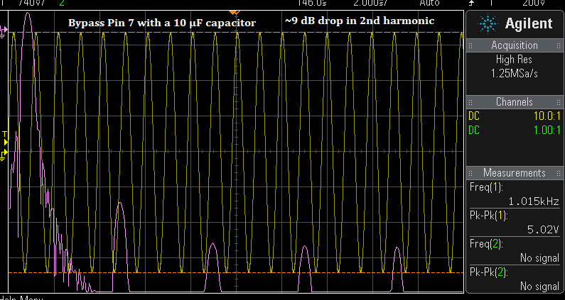
Above — An FFT of the PA driven to 697 mW with a ~ 1 KHz tone. Pretty good results from a single 2N4401/2N4403 emitter follower pair.
PA Instability
Once you connect all your AF stages together in a DC receiver, unwanted audio oscillations may occur.
This might be motor boating — a pulsed, typically low frequency oscillation that may even vary in amplitude and cause squegging. In addition to motor boating -- a steady, higher frequency oscillation tone that sounds hollow "or howls" may arise -- this usually occurs at loud volume.
I learned to think of your DC supply line as a highway connecting various stage inputs to outputs throughout your audio chain. Decoupling the DC line with series resistors and bypassing with AF and sometimes RF capacitors shunt to ground helps to stop AC signals from travelling along this highway. The ultimate way might be to use a capacitive multiplier BJT as shown on the first preamp labelled "one". The capacitor value connected to the base gets multiplied by the Beta of the transistor which sets a long time constant for very low frequency oscillations and those above this low corner frequency.
For motor boating, I normally place a 10-22 Ω decoupling resistor and
both a RF and AF bypass capacitor on the PA DC line. I suggest a 470-1000 µF for
the DC audio bypass capacitor as a minimum starting value. Each stage in
your DC receiver should get some low pass filtration with such an RC
network to keep AC signals from travelling down the DC highway.
Further, AF & HF oscillations may also occur in your PA voltage amp called the "VAS".
AF/RF oscillations also require low-pass filtration, but often just a local bypass capacitor alone will do the job. My PA emitted a ~ 800 Hz howling sound when the volume was turned up loudly. I tamed this by soldering a 270 pF MLCC RF cap from the emitter shunt to ground. For my guitar amps, I've had to apply other strategies.

Above — Ways to tame audio oscillations in a PA. The emitter degeneration resistor R1 could be increased to lower VAS gain. For example, from 39 to 47 Ω . And/or the C1 value could be increased to get the best result at high drive into the PA. This testing will annoy your family if you listen through a speaker like me! The VAS serves as the main PA voltage amp and offers a big source of instability in some PA designs.

Above — Additional circuitry I've used to tame a 40W guitar amp PA that oscillated at higher drive levels from AF to RF: 100 pF cap from collector to ground. then a 10 Ω resistor on the VAS collector with a RF bypass cap on each base followed by a series R at the BJT base terminal.
Interestingly in this DC receiver PA build, adding a Zobel network did nothing measurable, so I left it off. I've also connected the VAS base to ground via a series RC network. Sometimes, it's trial and error.
Voltage Amplifier with Active Gain Control

Above — The first version of the inverting active gain control stage. In my reference receiver, I employed the other half of the NE5532 as a follower/buffer. Technically, you do not have to use a buffer, but it helps isolate the active gain stage from the PA input. I've built other active gain control circuits that offer a better log response of the volume control, but this version seems simpler. If you need more maximum gain, drop R1 to 560 or 470 Ω etc..


![]()
I posted my longest video to date:
I'll post a few images from the video in the days ahead. Making such a big video felt pretty exhausting.
Best to you
![]()

Above — +/- 15 VDC input and ground ports on die cast chassis.

Above — Side view showing all the input and output ports.

Above — Schematic of 50 Ω differential bridge assembly. I employed a split DC supply to boost headroom and simplify op-amp biasing.I use the moderate power BD139/140 for the filter transistors: a sturdy part with low flicker noise -- no apologies.

Above — Input ports. Left: DC input (direct with a wire) using an SMA connector. Middle: AC coupled port with RCA jack. Built in 220 µF coupling cap allows testing of 50 ohm input Z audio amplifiers with no worries about the bridge causing a DC disturbance of the biasing or current.
Right: 50 Ω audio signal generator input with a BNC connector.

Above — The output of the instrumentation amp U1 gets buffered by the U2a follower. Low impedance output to use a 50 Ω terminated DSO as the detector.

Above — In analog output direct conversion or superhet receivers that use a diode ring product detector, we often employ a simple post product detector network that some refer to as a diplexer. It's not quite a diplexer, although, it does provide a 50 Ω termination to a narrow band of RF frequencies.
You might sweep this network at AF and RF with return loss bridges to study the input match versus frequency.

Above — My current post product detector network with part values chosen to try and match from 200 Hz to 200 MHz. This proved very difficult with such a simple network because the bandwidth is huge and really this calls for 2-3 networks to get it done. However, in simple receivers, this basic network works OK. The impedance match looks terrible from ~ 1 to 4 MHz, however, trying to fix this worsened the match elsewhere.
I performed the above AF measurements with my old audio return loss bridge built in 2010. It failed recently -- and that failure prompted me to design and build this new AF return loss bridge.
Compromise is a key term in simpler RF design. The network components shown gave me the best overall input Z match from 200 Hz to 200 MHz. This network also provided decent low-pass filtration of the RF lurking in the product detector's audio output. A 220 µF (or higher value) audio coupling capacitor helps keep the input noise down in the AF preamp.


Above — Testing gear used in the video: a 50 Ω Mini Circuits SMA terminator + barrel connector to 50 Ω coax -- and an RCA jack with a 2K potentiometer.

![]()
Above — This blog post supports the video shown above
[1] SIGNAL GENERATOR
Steve AA7U & Everett N4CY, built gear -- plus a procedure to test Intermodulation Distortion (IMD) on a loop amplifier using a Siglent SDG2042X generator and SSA3021X spectrum analyzer. Click on this hyperlink to read about it. I'm a fan of Siglent test equipment.
My strategy employs a 50.0 MHz crystal oscillator-based signal generator plus a 50.1 MHz VFO as the second signal source. My VFO tunes from about 49.6 to 51.8 MHz via a front panel air variable capacitor.
My 50.1 MHz VFO

Above — VFO schematic. Although I had worked out the low-pass filter L and C values, I built this VFO without a schematic and perhaps would build it differently if I needed to make another. I might consider tuning the output of the differential amplifier buffer for more output power and less harmonic energy.
I thought mostly about temperature drift when making this -- I started with JFET amp as the oscillator and struggled to make it work. This would be wise since a JFET offers better temperature drift over a BJT and gives a cleaner output signal with lower phase noise. However, I only had 1 day for this entire project and got frustrated. I deployed a common base PNP BJT local oscillator (LO) that never fails for me.
Both the LO and its buffer get regulated, well filtered DC. The LO gets temperature compensation/separation from the 8.2 volt Zener diode-based voltage regulator by way of 2 R C low-pass filters. I applied several C0G caps to resonate the tank and ran 2 air variable trimmer capacitors -- 1 as the main board frequency trimmer, the other as the front panel tuning control.
The LO gets lightly coupled via 1 pF to a differential amplifier emitter fed 10 mA with a current source. Differential amps offer strong reverse isolation, plus a reduced 2nd harmonic if the BJT balance is OK. The BC546 pair offer reasonable balance right out of the bin (without matching) & the BC546C serves as my go-to differential amp BJT from DC to ~ 100 MHz. The 10 mA current source, plus the 21 mA current in the final feedback amp provide heat for my temperature compensation scheme.
Low-pass filters built using T30-10 toroids worked OK. This was a board cram -- so the inductors are not spaced apart as much as when more board space is available. The 22 gauge air inductor measured ~ 374 nH & seems well anchored to the main 1-sided board with J-B Weld epoxy, plus the grounded coil lead soldered to the main board. The main board = 1/16″ (1.60 mm) Half Ounce 500 Series Copper Clad Board from MG Chemicals.


Above — Close up of the tank coil secured with a messy application of epoxy.

Above — Side view. The actual front panel capacitor leads were this long to allow slack to put on the herring tin cover. The Herring Tin lid added much difficulty with temperature compensation and construction tactics -- but I got it done! The idea of the herring tin cover came from this blog post

Above —View for the VFO showing the DC input port ( an RCA connector ) plus the SMA RF output port. 2 bolts hold the tin to the copper clad board.

Above — My 50.0 MHz xtal based oscillator next to the Herring made VFO. Ready for 2 tone testing. The front panel tuning capacitor is front left. The front panel bolt just fills in a hole I drilled by mistake.
If I want to drive a DUT such as a high IP3 amp -- or say a diode ring mixer ( I rarely use them anymore), I'll chain up 1 of 3 separate, sealed up wide band amplifiers that range from 12 dB to 26 dB gain (up to 150 MHz or so). I also have a plethora of low-pass and band-pass filters in sealed Hammond cases that go from 5 MHz to microwave if needed.
[2] 6 dB HYBRID COMBINER

Above — The VHF targeted hybrid combiner is also a return loss bridge and vice versa. No experimenter bench should likely be without a return loss bridge or 3. I built with standard 1/4 watt 1% metal film resistors and tried several different coils as the transformer. After many versions, I settled with 3 stacked BN61-2402 ferrites with 4 total turns of lightly twisted wire. I twisted the wires only enough so they would stay together during winding. Because of only 4 turns, I was able to use 28 gauge wire. I measured 43 dB port isolation at 50 MHz.

Above — The applied transformer.

Above — Boxed up combiner/return loss bridge with a Mini-Circuits Lab 50 Ω SMA resistive load attached.

Above — Another view of the hybrid coupler

![]()
Greetings! For 2-3 years, I’ve received emails from readers seeking a simple “popcorn” discrete transistor PA to substitute for the LM386 part in their DYI projects. Readers wanted 3-4 transistors maximum & no differential amplifiers with current sources — and hopefully low distortion up to 1 watt with a ~12 VDC single supply.
That seemed a tall order, but I did it (more or less). I’ll define ‘popcorn’ to mean that at maximum clean signal power, all harmonics are down to -50 to -55 dBc. This amp behaves well until driven to about 1.3 Watts. I made a video that lies in the last section.


Above — LM386 driven to 808 mW. This is the only LM386 scope trace I had where the voltage gain = 40 plus I had applied a good negative feedback network. Therefore, this practice seems a reasonable head-to-head test against the most venerable LM386. The Popcorn PA makes less distortion at 1 Watt, than the LM386 does at 0.81 W. At 1W power, the LM386 begins compressing into a square wave.
I promote bench experiments – and developed this amp on my bench. I began with a lower power version using 2N4401/2N4403 complimentary emitter followers to drive the speakers. Push- pull drive as opposed to a single-ended PA driver seems the best way to go for decent output power. You might substitute any number of small signal BJTS such as the 2N3904 for the 2N4401 (or the PNP equivalent) in this project.
Let’s start where I began. I’ll show the development of the Popcorn AF PA and give ideas to consider in your own experiments.
TABLE OF CONTENTS
[ SECTION 1 ] LOW POWER DEVELOPMENT VERSION
[ SECTION 2 ] OUTPUT STAGE BIAS
[ SECTION 3 ] FULL POWER VERSION
[ SECTION 4 ] VIDEO
---- [ SECTION 1 ] LOW POWER DEVELOPMENT VERSION ----
Above — The schematic of the initial & fledgling Popcorn PA using paired 2N4401/2N4403 as the complimentary emitter followers. In 1956 while working for RCA, H.C. Lin developed the first transistor power amp that didn’t use an output transformer. By around 1968, output transformers in solid state AF power amps had all but disappeared in professional designs.
Audio transformers suffer from non-linearity and in the case of the tiny transformers employed in cheap transistor radios of lore — these gave distortion, poor bass response -- plus very low output unless run in push-pull fashion. I suggest there are < 2 coherent reasons to use AF output transformers for solid state designs in 2023.
Input Stage
Without a differential pair as the input stage, I chose a PNP for the Q1 input amp with global negative feedback coming from the output rail going back to the Q1 emitter. The Q1 emitter also gets local feedback -- AC degeneration through the 330 Ω resistor. Because of all the feedback on Q1, Q2 provides most of the voltage gain and gets around double the collector current.
In all PA versions, Q1 bias gets set by a potentiometer (20K here). The pot proves necessary since all of us use a slightly different DC power supply voltages. The potentiometer allows you to optimize the Q1 bias for the lowest possible distortion with whatever DC power supply you use. When satisfied, you may remove the pot, measure it, and replace it with 1 -- or 2 series or parallel resistors to try to get as close as possible to the measured pot value. Alternately, you hard wire in a 20 – 25K trimmer potentiometer.
In the final Popcorn PA version, I show a fixed Q1 bias resistor and a procedure how to set this value
The Q2 “stack” includes Q2 & all the parts connected to the Q2 collector going straight up to the positive DC power supply rail. Q2 serves as the main voltage amplifier. I placed a 10 Ω emitter resistor as local negative feedback to stabilize the stack against HF during development. I have not found any HF instability in the Popcorn PA with or without that 10 Ω resistor.
With the 2K Q2 collector resistor, the stack draws ~ 2.5 mA. Let’s look at some DSO outputs:

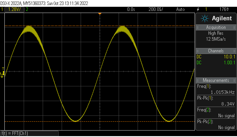
Above — DSO time domain output. The first draft PA driven to 2.01 volts peak-peak. Lovely sine wave. Power = 64 mW. 

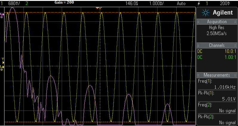
Above — Left PA driven to 4 Vpk-pk [ 253 mW ] and 5 Vpk-pk [ 396 mW ]. Only the fundamental 2nd,3rd and 4th harmonics shown. The 3rd harmonic tone starts to rise as the amp is driven to 4 Vpp. You can see the limitations of a single pair of TO-92 transistors such as the 2N4401/2N4403.
We’ve already exceeded the harmonic distortion goal for a popcorn PA amplifier. That is --- all harmonics must be down 50-55 dB at the maximum clean power

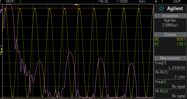
Above — FFT with PA driven to 6 Vpk-pk or 570 mW. The 3rd harmonic is only 27-28 dB down. These TO-92 transistors are getting hot and starting to stink. Some of this distortion might be Beta droop from the high collector current plus heat.
Regardless, this seems like unacceptable distortion. You could easily hit power level this high on a strong Morse code (CW) station.
At this point, the 2N4401/4403 emitter followers seem only good enough for headphone level listening.
What can we do to try boost their linearity?
Technique One — Bootstrapping


Above — The FFT of the PA driven to 2.0 Vpp or 63 mW into a 7.9 Ω load. If anything, the 3rd harmonic is about the same while the rest are a bit worse. Bootstrapping is not helping here.


Above — FFT of the PA driven to 6.03 Vpp or 753 mW. In this case, the harmonic distortion has improved. For example the 3rd harmonic improved by about 7 dB. But overall, the net distortion exceeds our harmonic distortion goal.
Theoretically, bootstrapping may help and often works as well as driving the Q2 stack with a current source. However, it doesn’t seem to work in this simple amplifier with a 2N4401/2N4403 pair.

Above — A fun FFT of what happens when you submit the 2N4401/2N4403 pair to 1 Watt power. Lots of compression, square waves & those emitter followers are smoking hot + stinking up the room.
Technique Two — Current Source


Above — For reference, With the 2K collector resistor driven to 3 Vpp. [142 mW power]
 Above — With 1K Q2 collector resistor driven to 3 Vpp. The 2nd harmonic improved by ~ 5 dB and the 3rd by about 4 dB. At higher power like 500-600 mW, , the distortion was still too high for my liking. Further, the increase in amplifier quiescent current for the net reduction in harmonic content wasn’t worth it.
I’ve gone as far as I can with the simple 2N4401/2N4403 emitter followers. I’ve got to add some current gain and get some proper power followers.
Before, we go to Section 3, the high power version of the Popcorn QRP PA -- Section 2 quickly covers output stage biasing:
---- [ SECTION 2
] OUTPUT STAGE BIAS ----
2 diodes produce a voltage drop of around 1.3 volts providing sufficient bias for the 2N4401/2N4403 output emitter followers. From reading & my own experiments, the output bias may affect PA output distortion. The most obvious way is by giving crossover distortion.


Above — An FFT of the 1 diode output bias with only the amp driven to 36 mW output power. The distortion dominates with odd order harmonics.

Above — FFT after adding back the 2nd output bias diode. This reduced the amplifier distortion shown above. Crossover plus output follower switching distortion pose factors we must live with. How far the output pair are biased from Class B towards Class A may also affect amplifier distortion.
However, using 2 diodes, we don’t have much control over that. You may place a small value resistor in series with 1 diode instead of using 2 diodes -- or in series with 2 (or more) diodes to change the output bias. An alternate way is to remove the diodes and replace them with a transistor.

[ SECTION 3 ] FULL POWER VERSION


Power Followers

Play with every resistor value on the test bench. You’ll probably make a better PA than I did.
Let’s go through some FFT’s of the Popcorn PA at various drive levels:


Above — Cranking up the drive! FFT while driven to output 8.39 or 1.11 Watts. Still meets our popcorn goal of all tones down 50-55 dB at maximum clean power.


Above — FFT while driven to 1.34 Watts. Things are falling apart. Ok, let’s finish up.

Above — It seems better to watch this video on YouTube directly.
Addendum:
To clarify, I think the LM386 is an awfully good part. Imagine if your design team made a linear IC that went into hundreds of thousands of projects or products? I'm a fan of the LM386 and the designers left us IC pins to add negative feedback with.
I cover this in the following blog post:
Link to my LM386 Experiments from November 2022
![]()
I should have this new project posted soon. Thanks for reading. Best!
![]()
This blog post arose from emails exchanged with a reader in 2015. The reader Frédéric — a newbie, sought to understand how the various sinusoidal oscillators worked in his circuits. He wanted explanations with little math & physics. Answering back, I realized how poor my basic oscillator theory teachings skills were. I studied up and wrote him a series of emails based on simple bench experiments. This Fall, I enhanced that content and even repeated many of the experiments. With joy and generosity, I present this content.
Introduction
Oscillators form the heart of radio frequency design & building. When you read oscillator papers written by genius electronics professionals, they might go something like this: They start off with the Barkhausen criterion & equations (of course). Then, they may veer straight into a series of equations using vector algebra complete with upper and lower case Greek letters; radians + total admittance in rectangular coordinates and perhaps more — all mixed in gruesome equations. Then comes the inevitable root locus plot, the showing of loop gain via a third-order voltage transfer function, and then finally they may go off into byzantine filter theory using complex conjugate poles. Absolutely fabulous stuff if you’re an engineer or physics major – and yes, I do exaggerate for fun.
All fun aside, understanding oscillator best practices ranks as problematic for some pros and amateurs alike since oscillators are non-linear circuits with linear aspects. You’ll find seemingly endless schematics to puzzle over. I’ve read that there are 18 or more variants of the Colpitts oscillator alone — spanning LF to terahertz.
Design & analysis of oscillators usually involves 3 basic methods:
[1] Negative resistance method using the +/-R & jX operators.
[2] Reflection amplifier method using scattering parameters & reflections (S11 and/or S22).
[3] Positive feedback loop method. This seems the easiest way for newcomers — I’ll only discuss concepts from the positive feedback loop method.
The 2 minimal conditions according to the Barkhausen conditions:
To oscillate + sustain: the input & output phase difference must be zero; and the whole loop gain must = 1 or greater than 1.
These are important minimal requirements. Real oscillator designers strive to achieve other goals that may include biasing for the best amplifier operating point, boosting resonator Q, lowering phase noise, and/or enhancing temperature + amplitude stability. They may work to reduce loading effects on the frequency determining circuit by the gain stage, or, perhaps, to fit the oscillator into a very tiny footprint. We’ll ignore all that stuff.
Let’s begin our minimum math discussion with the table of contents:
[ SECTION 1 ] Phase Difference
[ SECTION 2 ] Feedback & Function
[ SECTION 3 ] B E N C H E X P E R I M E N T S
via 3 basic types of frequency determining feedback networks
a. Transformer
b. Pi phase shifter
c. Tuned input and output
[ SECTION 4 ] Conclusion
[ SECTION 5 ] References
---------- [ SECTION 1 ] Phase
Difference ----------
Phase difference is the time interval between a discrete event occurring on 2 or more wave forms. The discrete event occurring at a point in time may be the positive peak of a sine wave, or perhaps the rising edge of a square wave, or something else. In electronics, 1 way to express time (phase) difference is in degrees.

Above — Two identical frequency sine waves. The discrete event in time is the positive peak of the sine wave. Wave A leads wave B. You might also say that B lags A. The time difference of these 2 events relates to the phase difference between the 2. This figure shows a very simple formula to help beginners.
Phase difference = the time difference between the discrete event in A and B divided by the total time of 1 complete cycle. That value gets multiplied by 360 to convert it to degrees. Thus, when total time = 1 second; if the time difference = .25 seconds, the phase difference = 90 degrees. If the time difference = 0, then the phase difference is 0 — & the 2 waves are said to be in phase.

---------- [ SECTION 2 ] Feedback and Function ----------
Feedback
A portion of the output signal (either a voltage or a current) is connected to, or “fed back” to the input. We'll focus on voltage feedback in this presentation.
Negative feedback
The fed back output signal has a 180 degrees phase difference with the input signal. This is called anti-phase, or inverted phase. Negative feedback bucks or subtracts from the input signal and gets called degenerative feedback.
Positive feedback
The fed back output signal is identical in phase to the input signal. This is called in-phase or a 0 degree phase difference (it may also be 360 degrees, or multiples of 360 degrees). Positive feedback adds to the input signal — it sums with the input voltage causing the output to increase and gets called regenerative feedback.
To sustain oscillation, the feedback must be positive since apart from power supply DC, an oscillator lacks an external input signal. The oscillator amplifier output goes to a buffer for external circuitry, plus, some portion of the output goes through a frequency determining network and back to the input with no net phase difference at the oscillation frequency. E.g., a positive feedback loop at 1 frequency.
A proper oscillator produces a repetitive output waveform. This output waveform may be sinusoidal (sine wave) or non-sinusoidal. We’ll focus on sinusoidal or near-sinusoidal RF oscillators that use LC inductor/capacitor circuits.
The oscillator as a filtered noise amplifier
Some impulse(s) must trigger the loop circuit to start oscillating. This might be turn-on noise, plus random noise from loop parts such as transistor thermal noise. That bit of noise loops around from output to input and starts the ball rolling.
Initially, positive feedback will cause the signal amplitude to build up and the active device will operate in it’s undistorted linear region. Eventually the rising linear oscillation amplitude will push the device into saturation and gain becomes nonlinear (distorted) & clipping + compression occurs. In its saturation region, amplifier gain tends to decrease as the signal amplitude moves towards the DC power supply voltage. At some point, the amplitude will reach steady state with stabilized or “limited” amplitude. The final amplitude depends on complex factors that may include the amplifier non-linear device characteristics and how deep into non-linear operation the gain stage goes.
Thus, at the loop frequency determined by the frequency determining circuitry, where the input and output phase difference is 0, a signal will arise having fundamental, harmonic and noise energy.
The loop gain criterion >=1 does not imply the amplifier voltage gain is 1 or 0 dB. The amplifier must provide enough gain to overcome circuit losses, plus have enough gain for start up — and to sustain oscillation in a variety of conditions such as adverse temperature or load changes. Further, losses may vary with the type of resonator circuit. A crystal or SAW resonator will give more insertion loss than an LC tank or pi filter at resonance.
Finally, the oscillator output harmonic distortion and stability is affected by the Q of the frequency determining network. A high Q circuit filters more sharply, so signals fall off from the resonant frequency more quickly than a low Q circuit. A high Q network also incurs less losses than a low Q circuit at resonance. The Q may also affect stability since non-linear amplifier function may vary with the degree of filtration offered by a given frequency determining network.
---------- [ SECTION 3 ] B E N C H E X P E R I M E N T S ----------
via 3 basic types of frequency determining feedback networks
[ 3a ] Transformer

Above — A common base BJT oscillator using transformer feedback. For the Section 3 experiments, I show minimalist, biased & functioning circuits at 1 frequency. By going with split DC supply, we enjoy a reduction in bias circuitry to allow a clear view of the frequency determining feedback network and amplifier. Each circuit employs a 10K resistor connected to the negative DC rail to provide a current source. All the circuits run between 0.8 to 1.3 mA DC current for easy comparison. To measure the emitter/collector current measure the voltage drop across either 100 Ω resistor and use Ohm’s Law to calculate current.
Above — To sample the output in my DSO, I placed 1 turn of wire through the T68-2 toroid & grounded 1 end. A 10x probe is connected to the hot end. Normally, we use a linear buffer with oscillators. Again, my approach is minimalist, so the basic oscillator circuit gets emphasized.


Above — A common gate version of the above oscillator.

Above — The DSO output of the common gate oscillator with lower distortion than the BJT equivalent. In general, like with tubes, JFET oscillators go into gain compression more gradually than a BJT, so oscillation amplitude regulation occurs with less distortion. Further, FETs offer quicker + better temperature stability, plus less heat dissipation into nearby circuitry compared to BJTs.

Above — An FFT of the common gate oscillator. The 2nd harmonic lies ~ 44 dB down. I found that the feedback coupling cap could go as low as 100 pF before it ceased to oscillate. From 100 to 200 pF the amplitude varied directly with the capacitor value. Above 200pF it made little difference to the amplitude up to 1000 pF ( the maximum value I tried with the coupling capacitor). This capacitor mainly serves to block the negative DC voltage flowing directly to ground through the secondary winding — AC coupling. In many oscillators, capacitors are used to AC couple circuits, but may also be part of the frequency determining network.
Discussion
Shown above is the classic Armstrong transformer feedback oscillator (also called the Meissner oscillator). The feedback gets coupled via an untuned secondary winding on the LC parallel “tank” resonator. The secondary gets called a tickler by some. Feedback networks maybe manipulated to provide the correct amount of feedback, provide a phase shift and also to impedance match the input to the output.
A common base/common gate amp runs a low input impedance and quite a high output impedance which the transformer turns ratio reflects.
The common base/common gate amp provides zero phase shift from the transistor input to output. In order for the phase difference at the oscillator amplifier input to be 0, the frequency determining network must also provide zero phase shift as shown by the phasing dots on the transformer primary and secondary. The tank, a parallel resonant circuit, is 1 all experimenters should know about. In summary, at resonance, XL = XC and the impedance is maximal (considered a pure resistance).

Above — The oscillator circuit with a common emitter (A) and common source (B) amplifier.

Above — DSO output wave forms for the (A) BJT and (B) FET oscillators. These amplifiers invert the phase of the signal from input to output (180 degree phase shift). Thus, the frequency determining network must also invert the phase. The parallel tank itself has 0 phase shift, so the secondary winding of the tank is where we perform this phase inversion. Note the polarity or phasing dots on the transformers.

Above — For newcomers to decode oscillators, a good place to start is to know whether your amplifier(s) invert the phase from input to output. A and B are op-amps shown in the inverting and non-inverting forms. When using logic gates biased as “linear amplifiers” we often employ inverters (a dead giveaway whether phase inversion happens). D shows the 3 equivalent BJT + FET circuits and whether they invert from input to output. This is something to memorize. If the oscillator contains 2 BJTs or FETs like in the Franklin oscillator, you identify whether each device inverts or not — and then trace the signal path though the loop.

Above — I built a version of the common emitter oscillator with too few secondary windings and the DSO results lie above. The oscillator starts, but then poops out because positive feedback voltage was too low in amplitude to sustain life.
On the other hand, if you make the feedback voltage too high in amplitude; depending on the amplifier type plus other factors, you may incur some bad side effects. This might include affecting amplifier input impedance and bias stability, loading the frequency determining network — or squegging. Squegging is more common in some oscillator topologies and/or oscillator amplifier types than others.
Essentially — undesirable parallel oscillations arise. A great example is motor boating in an AF power amplifier. Too much signal amplitude excessively charges the feedback coupling capacitor and this changes the bias of the amplifier in repetitive bursts. Keeping the feedback coupling capacitor value down as low as possible is an easy way to crush squegging in oscillators where squegging might occur.
Let’s move to the second type of frequency determining feedback networks: the pi network.
[ 3b ] Pi Phase Shifter
The humble ¼ wave pi network, whether made from L + C parts, or a transmission line such as coax or microstrip line serves as a fundamental building block in RF design. ¼ wavelength pi networks may function as impedance matcher, filter, phase shifter, frequency determining network, frequency controller, or a line balance converter just to name a few of its possible functions.
Those who work with antenna designs will get this — a ¼ wave coaxial matching transformer or stub can match a high impedance to a low impedance e.g. a capacitive reactance at 1 end may appear as an inductive reactance at the other.
The pi phase shifter is a representative feedback network for a bunch of famous oscillators. A high Q LC pi network at resonance (at its cutoff frequency peak) will function similarly to a bandpass filter. Studying the pi feedback network in the oscillators that follow may boost your insight into understanding many of the popular oscillators that are named after their inventor.
The frequency determining network of a Colpitts oscillator uses capacitive feedback, the Hartley uses inductive feedback, while the Vackar uses capacitive feedback plus a parallel LC tank. Further, these circuits may employ tapped capacitors or inductors to establish the correct feedback level at the oscillator’s amplifier input.
In a feedback loop, apart from the resonator components in a feedback loop, any stray inductance or capacitance from loop parts becomes part of the network. Of particular concern is the internal capacitances of the amplifier. Both FETS and BJTS have internal capacitances that vary directly with temperature — If temperature goes up so do these capacitances. The end result is frequency drift as temperature goes up and down.
Designers may work to minimize this drift by various mechanisms ranging from carefully regulated DC voltage to putting the oscillator in an oven chamber. With respect to our feedback network, they might try to reduce the impact of amplifier internal capacitance by absorbing or swamping this C with external capacitors in the feedback network. The aim is to minimize the effect of device internal capacitances in determining the oscillation frequency. For example, place a large capacitor in parallel with a nearby internal capacitance to absorb it.
I’ve read that from a frequency spectrum of DC to daylight, the theoretical phase shift range for a pi network is 0 to 270 degrees. So far, I’ve only built them with a phase shift from 0 to just over 180 degrees.
Above — A low pass form pi network phase shifter is added to a common emitter oscillator amplifier at A. I changed to using a 5 pF capacitor AC coupled to a 100K resistor as a load to measure across with my 10x probe (B). The RFC was just a random 1 mH epoxy-coated choke that was lying on my bench. I measured it at 920 µH. This choke serves only to prevent the collector AC output from passing though the 0.1 µF capacitor to ground and the value isn’t critical.
The CE transistor amp inverts the signal, so the feedback determining network must also invert the signal. The low pass form pi network serves as a metaphor to the Colpitts oscillator. I experimented with the feedback capacitor by placing a 5-450 pF air variable cap in its place and settled on 47 pF because it gave stable and sustained oscillation. Going below 40 pF ceased oscillation. If you change any value of capacitor or the inductor value, the output frequency will change.
The most common direct example of a low-pass pi style network phase shifter is that of the Pierce crystal oscillator shown as the inverting gate oscillator in an earlier diagram. The phase shift/frequency determining network includes a crystal functioning as the resonator. The entire feedback network also includes the output resistance of the gate.
Some logic ICs such as the 74HC4060 ripple counter; or any number of microcontrollers include an inverter gate so you may wire up an RC or crystal Pierce oscillator.


Above — Schematic and DSO measured output of a common emitter + high pass form pi network phase shifter. The network required an additional 0.1 µF AC coupling capacitor to prevent a DC short to ground through the left hand inductor. The series resonant frequency of that 0.1 µF cap = 6.6 MHz, so it provides a low impedance to the 7.35 MHz signal.
The high pass pi network version provides a metaphor to the Hartley oscillator. At their resonant frequency, many popular oscillator frequency determining networks resemble the circuitry & function of the pi phase shifter circuit in some form.

Above — A sidebar experiment using standard value series 100 pF capacitors that match a parallel tank to 50 Ω input & output Z at 7 MHz.

Above — A DSO trace of the above schematic showing a phase inversion. I had to tweak the frequency slightly to allow for L C variations from the design to get 180 degrees. The key point = RF filters using various topologies exhibit phase shift that changes with frequency within their pass-band, stop-band and roll-off frequency range in accordance with filter reactances & topology.
Applying L C networks, you may manipulate filter network impedances & reactances to get a desired phase shift at a particular frequency or frequency band.
Most oscillator’s seen in amateur literature are copies of someone else’s oscillator that’s kept exactly, or perhaps scaled to another frequency. This works fine in many cases. You may also figure lots out by performing experiments on your bench, or by pursuing computer-aided design & simulation.
Actually designing oscillators for specific goals requires math + measurement that goes beyond the scope of this blog post.

Let’s wrap up and go to the 3rd and final basic type of frequency determining feedback networks you might see in your travels.
[ 3c ] Tuned input and output

Above — A tuned input + tuned output oscillator or TITO oscillator with a common source amp. I had to tune the gate tank since its pretty difficult to match up 2 L C tanks without at least 1 variable capacitor.
The common source JFET amp inverts the signal. The TITO uses a bandpass filter phase shift network to invert the feedback signal back to 0 phase difference at the JFET input. The bandpass filter (called a 3 element pi section in my old ARRL handbook) gives the needed 180 degree phase shift.

Above — The DSO tracing for TITO.
[ Section 4 ] Conclusion ----------
I provided a basic, non-math introduction to RF oscillators using simple but functioning designs. The same principles apply to oscillators that use a crystal, SAW, coaxial, or MEMS resonator instead of an L C type circuit.
[ Section 5 ] References ----------
The Oscillator as a Reflection Amplifier, an Intuitive Approach to Oscillator Design,” by John W. Boyles, Microwave Journal, June 1986, pp. 83–98
Lindberg, E. (2013). Oscillators - a simple introduction. In Proceedings of ECCTD 2013 IEEE
M. Gottlieb, Practical Oscillator Handbook, Butterworth-Heinemann, London, 1997
R.W. Rhea, Oscillator Design and Computer Simulation, 2nd Edition, Noble, 1995
Yasuda, T., Uchino, K., Izumiya, S., Adachi, T., & Senanayaka, S. S. (2013). 433 MHz wide-tunable high Q SAW oscillator. 2013 Joint European Frequency & Time Forum & International Frequency Control Symposium (EFTF/IFC), 744–746
![]()


Spreadsheet taken down for re-location to another server.


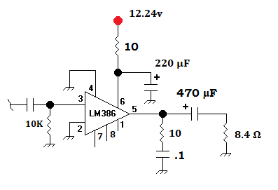
 Above — A basic power supply. The different green and orange LED resistors try to equalize their relative brightness on the front panel. 1 LED for each DC rail.
Above — For the first time ever, I'm using a commercial grade bridge
rectifier and will also apply this part in my high powered amps. You may
heat sink the GBUE2560 for high power amplifiers.
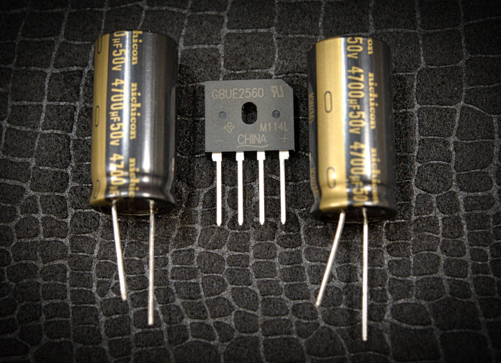
Above — Rectifier and 2 gorgeous reservoir caps for the DC power supply.

Above — The power supply transformer just sitting in the chassis prior to wire shortening and mounting.The Hammond 166L25 gives 12 watts out, while the166L20 gives about 8 watts clean output power. Further, if you regulate the op-amp DC supply with the 166L20, this means running +/-12 volts split as the unregulated DC voltage sags downs to less than 14 VDC on each rail when driven hard.

Above — The power supply section mounted and tested.

Above — My downstairs Telecaster ™ with a Seymour Duncan Phat Cat single coil pickup in the neck slot and his Alnico 2 Pro™ in the bridge position. I added my newly designed, switchable treble bleed circuit in February 2023.
4. Power Amplifier — P A —

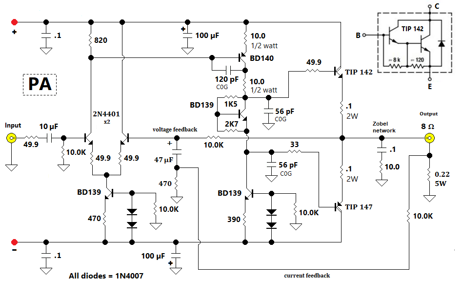
Above — PA schematic. I chose different transistors for the input emitter coupled pair and also for the finals compared to the original GAA -12 Practice Guitar Amp. Further, I sank a little more current in the emitter coupled pair and the VAS/driver stack. At this point, I only plan to run voltage feedback in the global feedback loop, although, I can easily add current feedback if desired.
I
measured a β of 540 for BC546B matched pair. The whole BC54-X- series
seem an incredible BJT collection offering low noise figure plus high β
and, of course, is long obsolete. I've got 30 pieces of the über low NF
BC549 in my parts bins for future 12 volt single-supply, discrete,
low-noise AF amplifiers.
Above — Notice from Mouser. The day after I installed the power Darlington complimentary finals, I got this notice by email. Obsolescence might be the central story of my electronic hobbyist career ? Happily, I've got enough genuine power follower pairs -- both standard and Darlington style to last me for a long time.

Above —The finals mounted in their heat sinks. Once again a hack saw helped fashion DYI heat sinks.

Above — The finals and PA mounted in the "cake pan". The power
transformer sat unmounted in this photo. Suzu with it smaller chassis and will go upstairs in our living room to serve as my main practice amp. The
downstairs GAA -12 amp serves as my main transcription amplifier. I
spend time downstairs transcribing horn solos. I rarely
listen to guitarists other than if a guitar happened to be on the song of the
horn player whom I'm transcribing. 
Above — Suzu's PA offers low distortion. I'm very happy with this PA stage. The matched input pair have obliterated the 2nd harmonic and I believe what's left are crossover + some intermodulation products from interactions with my outboard circuit, test leads, clips and probes.
I chose the Eminence Legend 1058 speaker for my upstairs practice amp.
Fortunately, many kind YouTube posters have uploaded head-to-head trials with various 10 inch guitar speakers for comparison. I tend to favour Alnico magnet 10 inch speakers, however, dislike their cost. My "non Alnico" preference seemed to the the Legend 1058 in several videos. So I bought one and found it well suited my purposes. — and the added bonus, it's not expensive.
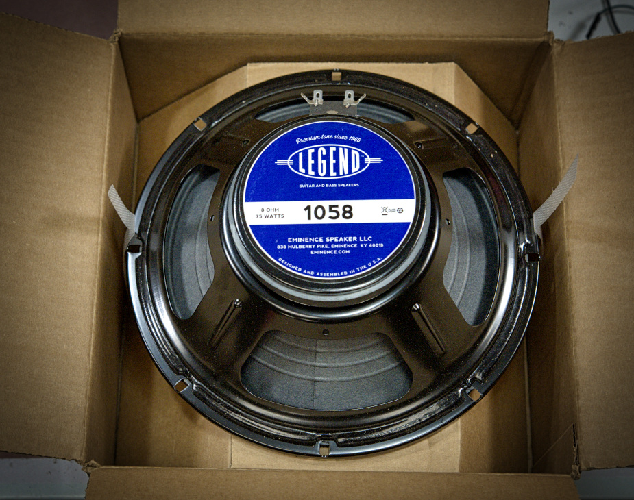

Above — The large dust cap makes the speaker look bigger than 10 inches in diameter. This speaker is a gem. Ferrite magnet and weighs 2 Kg.

Above — My wife designed & built a prototype cabinet from a plank of 12 inch wide, 3/4 inch thick pine. The final specs are 12 inches depth x 12 inches height x 14 inches width [ or 30.48 cm deep x 30.48 cm height X 35.56 cm width ]. I stuffed some fibreglass pink insulation in the cavity to dampen any reflecting waves. The back is partially open with a 2 inch gap across the top end. This keeps out cats (protects the speaker), keeps in the insulation and gives punchy bass tones with some room audio fill through he back of the speaker cabinet.

Above — I've got a Jensen Mod 10-35 in another identical cabinet at the moment. I like the strong mids for neck pickup solos better when compared to the 1058, however, it sound quite bright. It's best to listen to a speaker for many months before you write in in or off.


Best regards! Click here for my Guitar-Related Index


![]()
On a whim, I took another look at the LM386-4 one cold Sunday afternoon this November. My focus was to drive a loud speaker and not headphones. I won’t personally use the LM386 for a headphone amp as we enjoy so many better options. For example, an op-amp driving a pair of TO-92 followers, or perhaps placing 2 NE5532 op amps in parallel as the headphone PA stage.
Since the mid 1970’s the LM386 has enjoyed popularity amongst hobbyists for low to flea power AF power amplification. The NE612 mixer IC plus the LM386 have literally formed the basic building blocks of innumerable radio receivers amongst Hams and hobbyists for decades.
Although, imperfect like all other linear ICs, the LM386 design team delivered a simple, flexible, low power AF amp with reasonably low distortion.
This part is noisy though. The input noise density = ~ 50 nV/√(Hz) — about 10X that of an NE5532 op amp. So. if you use this part in high gain mode [with a gain of 100 to 200] and drive it with a low-level audio signal, you’ll really hear the noise (hiss) in your speaker.
Others online have provided detailed analysis about each stage of the LM386, so I won’t bother. However, I will comment about why it might be noisy. Normally, in modern AF power amps. the differential input pair emitters get 50 - 100 ohms of degeneration to boost linearity at the expense of noise. Other than that, in the IC only current sources connect to the emitters (and usually active loads to the collectors -- i.e. no resistors), However, the LM386 input pair get multiple large value resistors connected to their emitters. This translates into lots of Johnson noise from thermal agitation within conductors, plus related high-level input current noise that all gets amplified by the NPN voltage amp and delivered to the output stage.


1. Gain = 20 Mode
2. Bass Boost and More
3. Gain = 50 Mode
4. Gain = 200 Mode -- plus lifting and AC bypassing Pin 2
I'm avoiding math in 2022, as data shows that my blog readers don't care for it.

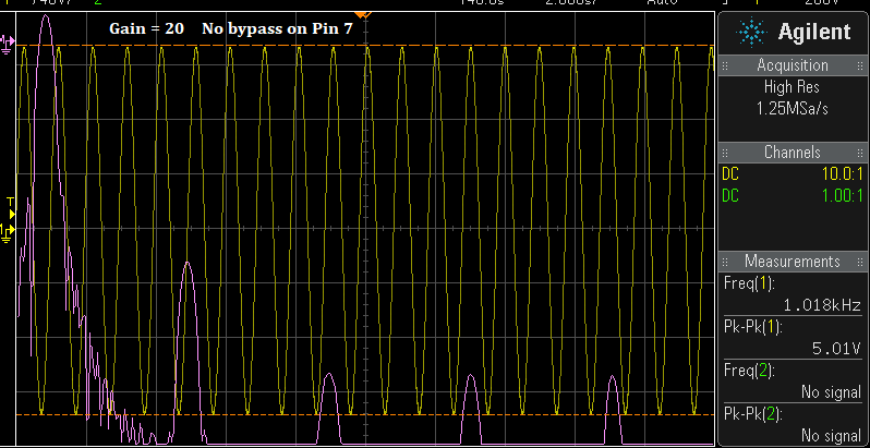


Above — I kept advancing the gain knob until clipping appeared on the top half.

Above — Switch to FFT mode, although you can still see the yellow coloured sine wave. At this point, the tones are almost level and 45 - 47 dB down. You may easily hear distortion at this level.


If you listen to this amplifier with music through a speaker, it sounds muffled and somewhat lacks the important mid frequencies for both voice and music. The hiss is definitely attenuated though. Further, the voltage gain goes from 20 without feedback down to around 8 with the 10K + .033 µF network added. There are other potential side effects to with such heavy feedback which I'll show soon.


Above — The bass boost circuit may produce weird distortion when driven hard in some circuits. The bottom half of the sine wave clips initially.

Let's adjust the feedback network and perhaps find something that works better.
In a classic PA with a differential transconductance input pair, 1 BJT base serves as the input stage while the other base receives the negative voltage feedback. The transconductance pair subtracts that negative feedback from the input and passes the difference voltage onto the voltage amplifier stage that follows. This doesn't happen in the LM386 -- negative feedback goes to the non-inverting BJT emitter which is often also the input side of the input emitter coupled pair.
Negative feedback also affects an amps gain, bandwidth, frequency response, plus its input and output impedance (although the output impedance is just fractions of an ohm). When we add AC feedback between pins 1 and 5, our network is in parallel with the 15K resistor and may be affected by other amplifier parameters including the gain and input impedance.
From the data sheet, In low gain mode, we should strive to keep the amplifier's closed loop gain 10 or greater which happens with the 10K resistor in our R C network. It's quite easy to turn your LM386 into an oscillator with too much feedback. I've noticed that feedback networks that look OK in SPICE simulations may actually oscillate in real life bench work -- especially with higher gain and/or drive.
I took the bass boost circuit example, kept the 10K resistor, and tried different capacitor values. If you lower the 10K resistor, you'll have to watch for oscillations at input drive levels high enough to cause distortion. This also may also reduce the LM386 voltage gain considerably.

Above — Our base schematic to evaluate different values of C1 and view the resultant FFT and voltage gain.

Above — FFT at 5 Vpp where C1 = 0.01µF. Outstanding results! This turned out to be the best feedback capacitor of the few I tried. The LM386 voltage gain dropped to just under 11 with that particular capacitor value for C1.

Above — Driving it as little harder to give 623 mW output power. Still fairly clean compared to other tracings.


Above — Pushed a little harder to 761 mW. Things are getting ugly. C1 still = 10 nF. Let's decrease the C1 value by a decade to 1 nF:

Above — FFT at 5 Vpp where C1 = 0.001µF. While not as impressive as when C1 = 10 nF, it's still quite good and the LM386 voltage gain is around 19.

Above — FFT at 7.14 Vpp or 759 mW output power, The second harmonic is somewhat better than the case where C1 = 0.01uF. 
Above — FFT at 5 Vpp where C1 = 470 pF. Another favourable reduction of harmonic distortion when the LM386 amp is running at reasonably high, unclipped power levels. I measured no loss in voltage gain with a 470 pF cap + 10K resistor.
I also tried a 220 pF cap - it worked somewhat, but the harmonic suppression started to fall off at this point. The overall best unclipped harmonic suppression occurred where C1 = 0.01 µF in my experiments, albeit with 45% voltage gain loss.
To decide on a C1 value, it's important to listen to it to with actual audio to ensure that any frequency peaks, or more importantly, the low pass effects caused by the network doesn't wreck the audio you listen to.


Above — FFT at 5 Vpp with a 1K2 and 10 µF cap between Pins 1 and 8. Although we see the 2nd harmonic at about 52 dB down, it's still OK for the LM386. Signal noise will appear louder compared to the "Bass Boost" feedback variants with the same output power.

Last section. Here's the famous schematic used by millions to make simple DYI audio projects:

Connecting Pins 1 and 8 AC bypass a 1.35K emitter resistor in the input pair -- and unleash the hounds. We get a full menu of gain, noise, and potentially harsh sounding distortion.

Above —In this separate experiment to showcase the worst-case scenario, I've manipulated & then pushed this particular amp into raucous distortion. Note the strong 3rd and 5th harmonics relative to the 2 even harmonics. This is worst case fuzz box stuff. While this might sound bad with your ears, it's great fun to see it on a DSO.
Above — Back to the main experiments using the schematic shown above... The FFT at 5 Vpp or 372 mW output power. The 2nd harmonic lies at -46 dBc.The various tones do not go down much at lower input signal levels.

Above — A slight increase from 7.01 to 7.09 Vpp. The 3rd harmonic is about 41 dB down.When in full gain mode, the LM386 tends to offers more odd harmonics

Above — Top and bottom sine wave clipping translates into wretched distortion.
My question -- will feedback similar to what we used in the Bass Boost variants lower the harmonic distortion?

Above — At our standard of 5 Vpp, the affects of feedback leap out at us. [ 10K plus 0.01 µF cap ] Feedback is our friend? However, the gain dropped to around 100 and you will hear lots of high frequency roll off.

Above — Vpp = 5 with a feedback network consisting of a 10K + 0.001 µF cap. The response is lack luster compared to 10K + 0.01 µF capacitor. The drop in voltage gain was only 2%. The 2nd harmonic is maybe 1-2 dB better than without the feedback network?


Above — There's an old trick left to try. Normally, most builders will ground Pin 2 like I did throughout this blog post. What if we AC couple Pin 2 to ground through capacitor C2?. This may help to better DC balance the input pair bases ( may reduce DC offset ) and perhaps even bypass some portion of the distortion to ground.
Does this work?

The bottom of the red line is the exact peak of the each tone with Pin 2 shunted to ground. Above the red line is the measured improvement for that particular tone caused by C2. I installed a switch across the C2 capacitor to make comparisons. . C2 = 0.01 µF in this particular experiment.
In my experiments with a gain of >=150 and no feedback network, when the LM386 is pushed into harmonic distortion, C2 lowered the harmonic tones by 4 to 8 dB. I tried C2 values of 0.01 to 0.27 µF
and changing the value of C2 within that range seemed to make no significant difference. Replacing C2 with a resistor of any value did not work to lower distortion.
C2 seemed to have less of an effect when the LM386 gain was lower than 150. At Gain = 20 with no feedback, I observed a maximum 2-3 dB maximal improvement in any 1 tone. With feedback, the effect diminished a little further, however, results were inconsistent. C2 does not appear to lower the harmonic distortion when the audio signal is unclipped -- rather, it seems to reduce distortion due to clipping when it happens.
I performed other experiments such as bringing the feedback to Pin 2 with Pin 2 connected to ground via a resistor or resistor + capacitor (like what you do with an op-amp or discrete AF amplifier). I also tried lowering the feedback 10K resistor value at various gain levels. Often enough, the result was that the LM386 would go into a writhing spasm when pushed into distortion. See below.

Above —Fancy feedback experiments often resulted in the above tracing. It seemed better to explore simpler ways to lower distortion.
Wow, this was a lot of work, but proved fun. I encourage you to perform your own experiments with the LM386. While no panacea, and a little long in the tooth, the LM386 reflects a simpler, mostly analog time for many of us home builders.
I suggest you consider using the LM386 with lower gain and build up your audio signal voltage with a low noise preamp using an op-amp like the NE5532.
Further, consider adding feedback [ 10K plus some value of C1 ] from Pins 5 to 1 and also AC coupling Pin 2 to ground. I did both of these tricks in my 2 photographed bench CD player listening tests shown in Section 2.
とてもいい
![]()
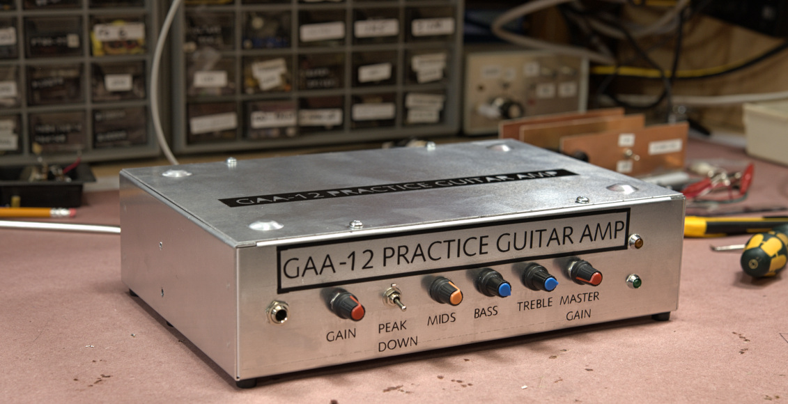
Greetings! This Fall, I built the first of 2 planned practice amps. Inspired by simple 1950’s tube guitar amps I too kept it simple. In those Golden-era amplifiers, you plug the guitar in 1 jack, the speaker in the other and hit the switch. Modern solid state guitar amplifiers with effect loops, frequency compensating gain control stages and features galore may just complicate things in the guitar - amp - player interface. While perhaps cool and fancy, these added stages may carry high-value resistors that boost op-amp input current noise and also increase resistor-related Johnson noise too.
My goal = make a low noise jazz / clean guitar amp as opposed to a low distortion, high-fidelity practice amplifier. I remember having to turn the volume pot on my Stratocaster to 0 between songs in my Marshall 50 - 100 Watt amp days of lore. The amp sounded great, but was super noisy unless the rest of the band was playing loudly to drown the amp noise out. At my age, a quiet amp seems desirable.
Note, I completely redesigned the preamp on November 15th after first posting this amplifier on November 6, 2022. Two things changed to trigger that : [ 1 ] I moved to 10 inch speakers [ 2 ], I moved to playing Fender Telecaster guitars 95% of the time instead of an arch top. With my back and wrist pain, the Telecaster proves much easier to play --- and also it's Leo Fender's gift to humanity. Such a joy to play. Thus, I re-designed my practice amp around playing a Telecaster through a 10 inch speaker. The result is a basic preamp with few AC coupling capacitors in the signal path.


Above — The maximum clean signal power into a dummy load with all harmonics < 60 dBC. Very happy.


![]()
Despite my rare posts — and sadly lacking much time for QRPHB, this blog enjoys reasonable traffic and I gratefully enjoy email from readers all over the world. Thank you !
Although home brew radio electronics remains a passion for me, component-level hobbyist radio electronics lies past its prime. Digital devices pushing ever higher frequencies = the new frontier as hardware plus software radio excites newer generations of builders. Craving simpler times, where we get to bias transistors and perhaps implement long-obsolete parts, some of us enjoy more nostalgic creativity — and prefer making radio gear from solid state parts.
Although I enjoy them all, it seems that many nostalgic ‘transistor plus resistor’ or tube RF circuits enthusiasts rarely seem to move beyond their comfort zone of LF - HF? I recall reading many wonderful VHF and UHF hardware projects in Ham Radio-related magazines in the 1980s into the 2000s. Where did this interest go? I do feel inspired by the modern-day Low Frequency Experimental Radio buffs who “get it done” despite the many challenges they face.
Perhaps ironically, we modern time solid-state builders enjoy an abundance of cheap, digital-based bench test equipment like never before.
QRPHB promotes hobbyist diversity and seeking knowledge. Like you, I’ve got many geeky ideas and interests and have way more questions than answers. We also champion inclusiveness – tribalism is tearing apart society. Whoever you are, whatever your hobby interests — this is a safe space to read, think and to question for all.
Lately, guitar amplifier-related hits dominate the blog. Please see a snippet of data from the past week below:

I’ve got many ideas to share and also much to learn about making jazz guitar amplifiers.
Here, once again, a small group of enthusiasts choose to make solid-state analog devices in a very tube dominated, plus digital guitar amp world. I think the best future home brew jazz guitar amps will involve digital, plus analog circuitry (and perhaps might include a single 12AX7) to give you that boss, sweet, bluesy guitar tone! In the distant future, after learning how, I will add sound bites on YouTube so you can hear my amps in action.
Behind the scenes at QRPHB live some amazing family members doing some cool but very geeky things. 1 particular area of interest for us is indoor air quality — specifically using data to test the effectiveness of our indoor air quality interventions such as filtration.

Above — Stuart's air quality system lying on the sand with a local admirer. Not many builders get wildlife inspecting their projects.

Above — A close up of Stuart's indoor air quality monitoring system. I feel amazed that we can measure particles below 5 microns --- let alone 0.3 µ
Here are a couple of URLs:
https://www.waveshare.com/wiki/Pico-Environment-Sensor
https://www.adafruit.com/product/4632
I’m also interested is radio astronomy and space weather. I like and support the GRAPE project:
SPACE WEATHER
Grape Version 1: First prototype of the low-cost personal space weather station receiver
pdf file for free download at
https://www.sciencedirect.com/science/article/pii/S2468067222000347
ABSTRACT
Crowd sourced data collection among the international community of amateur radio operators and shortwave listeners has great potential for addressing problems of under-sampling in the geospace system.
Quantitative Doppler measurements of high frequency (HF) time standard stations, used in bottom side ionospheric sensing, have been accomplished using existing radio hardware belonging to volunteers in distributed campaigns. However, typical shortwave receivers cannot be put to ordinary use while these measurements are being taken, do not have standardized signal chains, and are generally too expensive to be purchased for the sole purpose of taking Doppler measurements.
Here, we provide documentation for a low-cost intermediate frequency receiver, the Grape Version 1, which is designed specifically for measurements of North American time standard stations. Grape receivers can be easily constructed and deployed by amateur scientists in order to gain a deeper understanding of variations in radio propagation in their local environment. When compared over long periods and across distributed networks of stations, the resulting data yield insights on greater spatial and time scales. At the time of writing, several of these receivers have been deployed across the United States and are actively collecting data. These receivers form the first iteration of the Low-Cost Personal Space Weather Station network.
Gibbons, J., Collins, K., Kazdan, D., & Frissell, N. (2022). Grape Version 1: First prototype of the low-cost personal space weather station receiver. HardwareX, 11. https://doi.org/10.1016/j.ohx.2022.e00289
![]()
Introduction
Updated April 2, 2023 — scroll to the bottom for addendum
I love
working with analog ICs. For example, op-amps, sensors, audio PA chips — and of
course the parts we apply as modulators/demodulators and mixers for frequency
translation. Analog ICs using BJTs or MOS devices tend to contain 3 main
components: [1] differential amplifiers [2] various types of emitter or source
followers [3] constant current sources. In the case of bipolar transistors (which I'll write about), I use
the terms emitter-coupled pairs (ECPs) and differential pairs interchangeably in
this blog post.
Let’s focus on frequency translation with the so-called four quadrant analog multiplier that many refer to as the Gilbert cell mixer. Others may call it the Jones-Gilbert mixer since H.E. Jones had patented a similar layout prior to B. Gilbert’s 1968 paper [Reference 1].
It’s called 4 quadrant because in addition to 2 outputs, there are 2 inputs (X and Y) with 4 possible differential signal combinations: +X, +Y; -X, +Y ; -X, -Y and +X, -Y where +/- refers to the polarity of the AC waveform at the LO and RF inputs. A mixer switching transistor switches to an open or closed state by the polarity of the AC LO signal applied to its base.
Gilbert Cell Pros/Advantages
Gilbert Cell Cons/Disadvantages
Devices including semiconductors exhibit low frequency noise that is inversely
proportional to frequency that’s called 1/f, flicker, or contact noise. 1/f literally
means flicker noise is greater when frequency is lower. In the case of BJTs, this
low frequency voltage fluctuation (noise) likely gets produced when base
current flows through the rbb or base spreading resistance of the mixer ECPs
and interacts with microscopic contact + surface imperfections in the
substrate.
Flicker noise adds to the mixer noise figure and proves even more vexing with
direct conversion architectures since these mix down to audio frequency — and any low
frequency base band noise (such as flicker noise) gets amplified in the audio signal chain. Flicker noise is
worse in Metal Oxide Semiconductor (MOS) transistors than in BJTs [Reference 2].
Modern Gilbert cell mixer engineers toil relentlessly to reduce flicker noise / mixer noise figure at very high frequencies.
Gilbert Cell Cons/Disadvantages continued...
I do not make superheterodyne receivers and instead focus on the direct conversion architectures of zero-IF or low-IF. Thus, an IC such as the SA612 would make a poor choice for me on the Ham bands since I like to listen to CW pileups on contest weekends where in amongst weak signal clusters lie abundant strong signals that would invariably overload my low power IC product detector(s) and make me feel sad.
Then, too, an analog Gilbert cell IC might be OK for use in a DC receiver used to study the atmosphere or listen to decametric emissions from Jupiter.
Double balanced
The Gilbert cell mixer is double balanced for LO and RF so, ideally there should be no LO or RF leakage into the outputs. In reality, port isolation isn’t perfect and factors including BJT matching and single-ended versus balanced LO & RF inputs may affect port isolation along with other mixer parameters such as IP3. However, the Gilbert cell mixer does not just rely on transformers to give balance; therefore, it still functions as a double-balanced mixer whether you use single-ended or differential inputs on the LO and RF ports
Mixer balance affects port to port isolation and more. When unequal currents flow in an ECP, overall cancellation is reduced. Symmetry is everything in balanced mixers — common mode noise, input signals & even order harmonics alike get reduced in amplitude through precise 0 to 180 degree phase shift cancellations within the ECPs of the Gilbert cell mixer.
Going… going… Gong!
Many classic Gilbert cell monolithic IC mixers lie obsolete. These include the MC1496, MC1595, IAM-81028, SL6440, µPC1037, SOP42, TL-442 and AN612. The NE/SA 602 or 612 chip is still available but must be circling the drain at this point. Still in production IC packages range from the simple HFA3101BZ96 to the ADL5801-5802, ADL5380 (I/Q demodulator), MAX2680-MAX2681-MAX2682, SMA5101 and many others.
Like they say — “if you like an analog part now, buy some today because they might not be around in the days past tomorrow”. It's worth reflecting that industry needs dictate the rise & lifespan of parts. Hams and hobbyists latch on to certain parts while in production and well after they turn obsolete —but it was never about home brew electronics.
Modern
builders have employed Gilbert multiplier cell mixers into mm-waves in industry
or research. Apart from BJT and MOS devices, in microwave you might see monolithic
microwave integrated circuit (MMIC)
implementations in InP HBT, SiGe HBT, GaAs HBT and pHEMT high speed technology.
Modern Gilbert cell mixers typically employ low DC voltage, low to moderate
current and very high speeds.
Predistortion and improving linearity in the ECP
Barry Gilbert’s version of the 4-quadrant analog multiplier predistorted the LO input signal of the switching transistors by essentially using diodes to compress the signal logarithmically. From his 1968 paper describing his experiments, the terms Gilbert cell or Gilbert mixer arose to popularity [Reference 1].
For amateur radio buffs, we may eliminate his linearizing predistortion circuitry plus any DC offset balancers since as a RF mixer we employ high Q, tuned band-pass circuitry to remove unwanted frequencies — and as a product detector we use a low-pass filter network to remove any residual carrier and other RF garbage that leaks through to the zero-IF or low-IF output(s).
The 4-quadrant multiplier proves a versatile analog workhorse circuit
The versatile 4-quadrant multiplier may be set up to function as a squarer/multiplier, divider/square rooter, frequency doubler, balanced modulator or demodulator for AM or SSB, an FM quadrature detector and a variable gain control amongst other tasks. A true analog workhorse circuit.
Gilbert Cell Mixer Function
Let’s examine basic mixer function.

Above — The basic structure of the Gilbert cell mixer. LO is applied to the X ports and RF to the Y ports.
The switch quad (sometimes called the mixer core) Q1- Q4 multiply the linear current from Q5 and Q6 with the switched LO signal. Q5 and Q6 provide +/- RF current and Q1 and Q4 switch alternately to provide normal or inverted output to the Q1 load resistor while Q2 and Q3 switch alternately to drive the Q4 load resistor with a normal or inverted output.
Switch quad [ Q1-Q4 ]
2 cross-coupled, parallel, differential BJT pairs form a quad switchTransconductance pair [ Q5, Q6 ]
Simple bias resistor versus constant current source
The ideal current source offers a fixed current level, a high output resistance, & low noise.

Figure 2 for Discussion Figures A to D show the (lower 2) simple differential amps with a split DC supply for clarity.
For maximum real-world performance, IC designers use ECP’s matched for VBE and hFE (Beta). That’s much easier to do when the transistors come from the same substrate. If you choose to build a Gilbert cell from discrete BJTS — indeed, you should match the discrete transistors that make up your ECPs.
With some ICs, you'll decide whether to use a plain old emitter resistor to provide ‘constant current’ to your mixer, or to employ a constant current sink device: a transistor biased with resistors and/or diodes, or used to mirror a separate reference current.
In Figure A, RE is a simple resistor and the current flowing through the ECP is determined by -VEE and RE. The sum of the currents flowing through each ½ of the ECP should ideally be fixed or constant. In order for that to happen, RE must be a large value resistor to drop a significant voltage across it.
This means the corresponding DC voltage must also be large. Typically, most builders run lower DC voltages such as 5 to 12 volts with a single power supply rail. Thus, RE falls short as a constant current source whether running single or split DC supply. It might be perfectly OK to run RE in bench design work, for low complexity radios, and/or at very high frequencies.
Figure B
shows RE replaced by a transistor Q3. We assume that the collector to emitter
current of Q3 is equal to the base to emitter current X the current gain of the
transistor & its current gain is independent of the collector to emitter
voltage.
Figure C shows Q3 fully biased from the negative rail with included diodes
to boost temperature stability. Since the diodes get fabricated from the same
wafer, they thermally track the ECPs and offset temperature-related current
changes.
While Figure C is OK, some constant current sources are better than others. A
basic, better-grade and popular constant current source biased with positive DC
is shown in Figure D. This circuit is known as a current mirror and a ‘diode-connected’
BJT (Q3) forms the current mirror. Just like ECP’s, both current mirror
transistors need matching for best results.
Various forms of improved current mirrors exist and include for example, the
Wilson and Widlar current mirror designs. You may see emitter resistors on both
transistors to help with transistor matching and to raise the effective
collector resistance. Finally, please refer to Figure E to see cascaded current
mirrors in use with a Gilbert cell mixer. An example of this lies in the MC1496.
Input signals common to both differential amplifier inputs (common mode signals) such as noise, or stray voltages that drive both inputs will not get amplified since this is a difference amplifier. In effect, the differential pair rejects common mode signals — and the better this rejection, the better the balance of the differential stages are in the amplifier or mixer. Thus, DC current through mixer ECPs should ideally remain fixed no matter what— and a constant current source helps achieve this. Other Gilbert cell mixer constant current source benefits might include improved output linearity, boosted port isolation & potentially reduced power rail noise.
Thus, a constant current source marks a big improvement over the plain old resistor RE. Summarized --- For an ECP, the higher the resistance of its current source, the lower the common mode gain + the better the common mode rejection ratio.
I have merely scratched the surface about constant current sources. Abundant constant current source info lies in books on differential amplifiers + constant current sources and on various web sites.
Balanced or unbalanced input and/or output
We’ve got decisions to make. Considering the external RF or LO stages that drive our Gilbert cell mixer – plus whatever stage is going to receive the mixer’s output, we’ve got the following choices:
[2] Mixer Output Ports
I favor differential output using a center-tapped transformer which doubles your output power over a single ended output. However, then you’ve got to make or purchase a center tapped transformer that will also step down the high collector impedance to something close to your post transformer device input impedance. This might even involve you winding a trifilar transformer on a ferrite toroid. Many experimenters evidently suffer an inflammatory disease known as TTA [ Trifilar Transformer Allergy]. For them, a trifilar transformer crosses the line.
Wouldn’t it be easier to just apply a simple resistor to convert that collector current into a voltage and then not have to mess with a transformer? Yes. There are always trade-offs — plus your needs may vary. What are you using the mixer for? If it’s just a transmit mixer, I may just use a resistor and feel OK with dropping my conversion gain by half. But that might not be OK for a receiver. Since a major reason to employ a Gilbert cell mixer is to get mixer conversion gain, I tend to go with differential output to either a single ended or differential input next stage in my receivers. Your needs may vary.
Datasheet Studies
Let’s dive in. I’ll briefly show 3 data sheet examples that illustrate single supply DC biasing with or without constant current sources and various mixer input and output strategies.
Recall that the RF enters via a differential transconductor with their output currents commutated by a quad of LO switches. The top switch quad operates in the saturation region while the bottom ECP are biased in their linear region.

Above — The data sheet schematic of the S042P Gilbert cell IC. No constant current source. Typical current consumption = 2.15 mA. No internal switch quad collector resistors are provided. The resistors and diodes shown above are contained in the substrate. The builder supplies external bypass/signal capacitors, gain setting resistor(s) for the transconductance pair current — and AC connections through coils for the RF, LO and output in typical applications.
This DIP-14 IC mixer offered by Siemens Semiconductors (Infineon) ran a maximum DC voltage of 15v and went to 200 MHz. It featured an optional built-in oscillator. The data sheet shows a NF of 7 dB. They also offered a round, leaded, metal case version called the SO42E. You’ll see this IC in many European home brew gear, including the projects of LF and VLF enthusiasts in more recent times. The oldest schematic I could find using the S042P was dated 1979.
Using an 8K2 instead of an 8K resistor, I show the upper quad plus lower ECP DC bias voltages using a bench DC supply of 12.18v. The entire bias stack consumes 1.2 mA. The wafer fabricated bias diodes are thermally matched to the ECPs in this IC for temperature compensation. This data sheet shows an archetypical way a builder may bias a discrete transistor Gilbert cell mixer. Each diode in the bias stack drops ~ 0.61 VDC.
The diode pairs may be replaced by fixed resistors and biasing via resistor voltage dividers plus the 2K2 and 3K3 decoupling resistors remains common in home brew BJT Gilbert cells built today.
Since the transistor fT’s were high (probably >=1 GHz), VHF oscillations often occur. They suggest a 10-50 pF capacitor between the LO inputs to prevent VHF parasitic oscillations. Other builders implemented low value series resistors on the ECP base inputs as well. 
Above — A data sheet schematic of the HFA3101 Gilbert cell IC with some DC bias values added by me. No constant current source. Absolute maximum current consumption = 30 mA. This is just a very fast transistor array with a small PC board footprint. The builder supplies all biasing resistors, capacitors, & current setting + degeneration resistors for the transconductance pair — and AC connections through resistors, caps, and/or coils for the RF, LO and output.
This SOIC-8 IC mixer offered by Renesas specifies an fT of 10 GHz. It’s tiny and fast using BJTs! A review of the data sheet proves fascinating. This part appears well characterized for 50 Ω use and the circuit examples give clues how we can set up our own discrete or IC mixers using single-ended inputs and outputs. The singled-ended LO + RF input penalty of reduced port isolation is acknowledged in the data sheet and it well shows the trade-offs builders must consider.
At high frequencies such as UHF, they specify that the LO must be matched to the switch quad input to avoid parasitic oscillations. RF port matching also proves important for conversion gain. Clearly a mixer operating as a upconverter @ 825 MHz is a whole different animal from a HF Gilbert cell mixer. The design examples show very low value biasing resistors — again this is for UHF and I estimate the low values may provide stable bias, low noise, low input impedance and decreased potential for parasitic oscillations. My added notes show a VCC of 2.96 VDC. I swapped a 120 Ω resistor for the 110 Ω resistor shown. DC bias voltages are shown for the upper quad and lower ECP — the total current draw of the bias stack alone = 4.4 mA due to the low value bias resistors.
The RF capacitor values shown don't make sense. The series resonant frequency of the 0.01 µF caps shown seems too low for UHF applications.
Also mentioned in the data sheet, when a (single-ended) output tuned coil is shunted with a 2K resistor, this improves the third order intercept while somewhat decreasing gain. E.g. less distortion products are generated while stability is enhanced. This would be something to try at HF on your test bench if you’ve got the test gear and want to run a tuned, single ended output.
You really go to school by reading this data sheet. What a fabulous IC that doesn’t use MOS transistors — so we can relate to it a bit better.

Above — The schematic of the silicon BJT MMIC IAM81008 Gilbert cell IC offered in the past by Hewlett Packard (Keysight Technologies). Single polarity bias supply of 4 to 8 VDC [ most often builders would use 5 volts which would draw a maximum DC current of 12 mA. SSB NF = 17 dB. RF and LO ports = 50 Ω. 8 dB RF to IF conversion gain from 0.05 - 5 GHz with an IF output from DC to 1 GHz.
This is a great historical example of a complete, active mixer that required minimal off-chip parts to get it operating at VHF to UHF -- plus it also featured an interesting on-chip bias circuit. You just need to AC couple in your RF plus LO signals with appropriate value capacitors -- and then provide a VCC and ground. Pretty amazing active 5 GHz IC mixer in that day in time.
As such, this double-balanced mixer was used with single-ended LO + RF and output ports. A built-in emitter follower reduced loading effects on the output port, The current sources schematic numbered 1,2 and 3 show the evolution from a typical on-chip current mirror to something much more sophisticated.
This mixer seemed popular for VHF and UHF work in Europe for experimenters and while it suffered from a relatively high NF (lots of transistors + resistors) and low dynamic range, it worked OK as second mixer in a typical receiver -- or perhaps as a transmit or PLL mixer.
Many writers have covered the SA-612 and ilk, so I won’t. For me, a measured SSB NF of <= ~8 dB at <= 45 MHz made that part special when it came out. However, modern Gilbert cells ICs offer a much improved dynamic range plus a higher upper frequency limit — although they’re not as easy to use for HF to lower VHF home brew experiments as the popular SA612.
Home brew Gilbert cell Mixers
Although this blog post covers analog ICs, I'll write a few comments about making home brew versions with discrete transistors. I've built at least 6 discrete BJT home brew Gilbert cell mixers and each of them suffered strong parasitic oscillations between 110 to 430 MHz. Whether using single-ended or differential inputs or output, they oscillated. When running higher currents such as > 12 mA to get a better input intercept, parasitic oscillations tended to worsen. Some mixers were stable with 1 set of LO and RF input frequencies, but then became unstable when used with different LO and RF input frequencies. Quite vexing.
I had to spend a lot of time adding series resistors, bypass capacitors and so forth to swamp out these VHF-UHF oscillations. The whole process proved time consuming and frustrating. With commercial, analog IC versions, I did not suffer these problems, or they were easily fixed if parasitic oscillations happened to arise.
I can make a simple, stable, active, transformer-balanced home brew mixer with 2-4 FETs or BJTs that will outperform any of my discrete transistor Gilbert cell mixers with far less parts and stress. Thus, I tend to use commercial IC Gilbert cell mixers.You may have better luck! Perhaps, I'm doing something wrong?

Above — A spectrum analyzer screen shot of the output of 1 of my better home brew Gilbert cell mixers. RF = 14.08 MHz @ 0 dBm input, LO = 9.98 MHz @ 0 dBm input. This was for a down conversion mixer to a 4.06 MHz IF. RF conversion gain = 16.35 dB. I've measured as much as 19 dB conversion gain in my home brew Gilbert cells once parasitic oscillations were stifled. The LO and RF signals are down ~ 32 dB which shows pretty good balance for a home brew Gilbert cell mixer. You can see other strong tones in this image, but those are pretty standard in RF mixers. This was an OK mixer.

Above — The spectral output of a Mini Circuits Level 7 diode ring mixer for comparison. Conversion loss = ~ 6 dB at 4 MHz. Beautiful suppression of the LO and RF input signals. In my home brew diode rings, I usually get only about 35 - 40 dB RF and LO suppression due to mismatches in my diodes + transformers, and from layout asymmetry.
Update April 2, 2023 - - Discrete BJT mixer - -
I developed a very stable Gilbert cell mixer that uses no transformers in March 2023. I've run it from 2 MHz up to ~120 MHz with no VHF-UHF parasitic oscillations.
The input LO and RF are well defined at VHF and = 50 Ω. The output impedance is low and easily matched to 50 ohm input devices with a resistor or pi match. The Q4 collector resistor at 1.5K gave the best conversion gain, but this value may go as low as 1K Ω.

Above — The IF output at 10.7 MHz. I used the BC547 CTA transistor for the emitter coupled pairs. This transistor consistently gives outstanding balance despite not matching my differential transistor pairs.
Above — My experimenters Gilbert cell mixer showing the variables such as capacitor choice versus frequency, setting up the 2 voltage divider bias networks, choosing mixer current & emitter degeneration to affect the input intercept. The BC547C specifies an fT of 300. Thanks.
 Above — Yet another experimenters circuit for HF.
References
[1] B. Gilbert, “A precise four-quadrant multiplier with sub nanosecond response,” IEEE Journal of Solid State Circuits, Vol. 3, No. 4, December 1968, pp. 365-373.
[2] Syu, J.-S., Meng, C., & Wang, C.-L. (2013). A 2.4-GHz Low-Flicker-Noise CMOS Sub-Harmonic Receiver. IEEE Transactions on Circuits & Systems. Part I: Regular Papers, 60(2), 437–447
![]()
Above — Our 2 lab supervisors
Please subscribe. Going forward, I'll rely more on videos as people like them.
The resource I lack the most is time.
— Update —
I sincerely thank you for your support!
Over 90 QRPHB Bench Tour video views in 2 days and 52 YouTube subscribers.
I feel amazed as I really have not posted much content in the past few years --- and do not promote QRPHB whatsoever. Best to you!
![]()
For Season 24, after a hiatus from RF, I plan to share some radio projects beginning in late October.

Above — I've cleaned up my bench and began ordering some RF parts so they'll be here for Fall experiments. This summer, countless people have emailed me and requested some RF content, so I'll oblige. After a few years away from RF experiments, I feel reinvigorated. I've kept up my reading, but not RF bench experiments --- plus I'll have to brush up on my lab procedures.
In addition, I just got a modern camera to add some video content to my blog posts. Therefore, I've got to learn V logger stuff and choose plus learn how to operate some video-editing software. That will take time. Time is the 1 resource I lack the most and I'm jealous of those retired experimenters who have time to work on stuff at their leisure. My experiments occur late at night with a push-through-to-the-end philosophy.
Until then, here is a gardening topic. I'm an avid gardener and for me it's served as my mental health re-constructor over the past ~ 3 years.
Single Dahlias
I Iove Dahlias and so do the pollinators around our place. We have more solitary bees than honey bees and I’ve taken measures to provide them a variety of spaces to nest in and around our property.
I mostly grow single row Dahlias for these pollinators and actually the so-called "single row" collection can be divided into Anemone, Collarette, Orchid, Orchette, Single, Micro-Peony and Species (non-hybrid) Dahlias. Unlike the fancy modern hybrids that people grow for weddings and for beauty, "single rows" have just 1 basic row of petals and their private bits are exposed so pollinators can easily access their pollen and nectar.
2 examples of species plants include Dahlia merckii and Dahlia apiculate. I grow the latter.
I wanted to share my adventures with an Anemone hybrid that I’ve worked with for 2 years. My basic plan is to get a variety of seeds, germinate them in late February under lights, grow them indoors until the frost is gone and then plonk them in our gardens. If the plant performs well, then continue that line by saving the tuber, and perhaps growing-on some cuttings for next season.
I’ve noticed that all my "single row" Dahlias struggle in the scorching sun of late June to middle August. I planted some in a shady garden and the flowers plus foliage stays much nicer during the record setting, super-hot summer sun we got in both 2021-2022. In that shady garden, flowers get about 6-7 hours of sunlight then dappled shade to full shade.


Above — The seedlings on Feb 28, 2022. The largest seedling is the flower I'm describing. I had to re-pot it twice before planting in in our full sun front garden on May 17th. It started blooming in the house while sitting in a south facing window.


Above — Photo taken today, Sept 4, 2022. In late July into middle August, the leaves got scorched by the blazing hot sun during our heat wave. Many of the flower buds "cooked". They did not flower, rather they were burnt & turned black. I cut off these dead buds. This was not due to lack of water and a good mulch at the base of the plant — our hot weather has been brutal for the past 2 years. For awhile, there were very few flowers on this plant.

Above — The plant continues to recover and once again transformed into a flower machine. In addition, these flowers last longer than other "single row" dahlias in our gardens. This 1's a keeper and serves as a bee magnet. Grown from 1 seed this year, it out performs our other tuber-grown Dahlias in terms of bud production. Last year, we had the first frost kill of our Dahlias on November 3rd.

Above — Take care of yourself. Connect with nature. It will help clear your mind so you can do some serious electronics. Best to you!
![]()
I quickly evaluated a MCL or Mini-Circuits Labs TC1-1-13M+ transformer as a balun. Although we live in a single-ended dominant RF world (single-ended LNAs, IF amps, bandpass filters, low-pass filters, VFOs, VCOs, etc.) there are times when you want differential output. That’s 2 outputs inverted, or 180 degrees apart with hopefully equal amplitude in each arm.
It’s easy to make a homebrew balun, but I wanted to see how the MCL part compares to my home-built stuff which might be 4 or 5 twisted turns of #28 AWG on a FB-43-2402 binocular core, or something like that.
The MCL part looks tiny and its small footprint [ 3.81mm X 1.65 mm ] would well suit my hybrid SMT/through-hole build style using Ugly Construction with a few carved copper islands for the SMT parts and AC input/outputs, or DC inputs. I prefer my homebrew projects to be as small as possible.
MCL specs this part at 50 Ω port impedance from 4.5 to 3000 MHz. An amazing wide band response. I measured the inductance of each arm at 21.6 µH. This is about the same as 4 turns through a FB-43-2402 balun I had lying around in my ready-made transformer tray. Some of these transformers are really sketchy and have been soldered in out of quick bench experiments in some cases for over decades.
My current interest is for lower HF, and in particular, ~7 MHz.
URL for the TC1-1-13M+ data sheet: https://www.minicircuits.com/pdfs/TC1-1-13M+.pdf

Above — The schematic of my testing jig.

Above — The MCL output into both 50 Ω terminated channels of my DSO with a 7.039 MHz signal applied. The phase difference is perfect as shown and lies in spec at all frequencies I tested -- really amazing. The amplitude difference isn't as good at HF but was within spec at lower VHF and all the way to ~3 GHz.

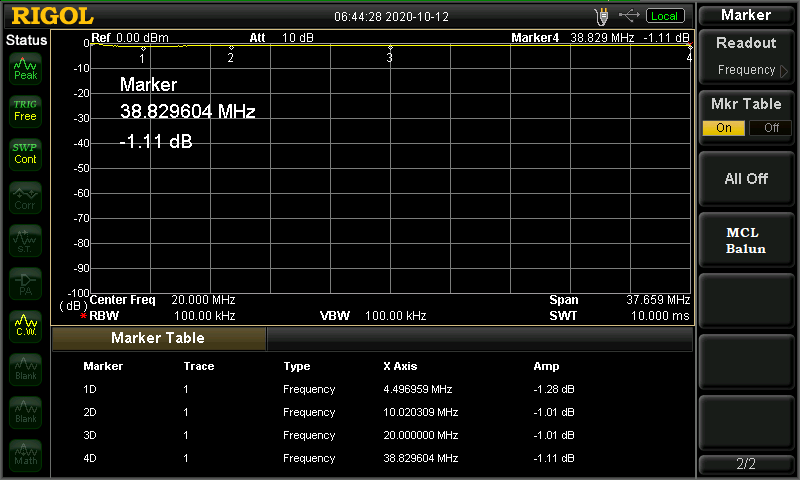

Above — The sweep of my balun with identical settings.The #43 mix ferrite material rears its ugly head. ~ 3 dB insertion loss that gets worse as you move up into VHF and above. I've only got #61 and #43 material ferrites for making transmission line transformers. C'est la vie!
It's fun and humbling to compare your homebrew parts against premium industry components.
Ciao
![]()
In 2022 I l stopped most of my subscriptions to magazines and journals. I've got 2 left:

Above — I've belonged to Radio Amateurs of/du Canada for over 3 decades. The quality of our RAC journal 'The Canadian Amateur' has grown — and the build + technical articles rank as first class.

Above — Having subscribed to Nuts and Volts for many years, I still enjoy reading each new issue online. It helps keep me up-to-date with the hobbyist forefront. My interests aren't confined to amateur radio; they include a spectrum of electronics-related topics and general sciences.

My main hobby in Spring|Summer:


![]()
The story of life as a hobbyist builder --- you get this email from a vendor from whom you buy parts:

![]()