Normal view

There are new articles available, click to refresh the page.
Before yesterdayHam Radio Blogs

Some useful equivalences of very short very mismatched transmission lines

By: Owen
31 July 2024 at 16:12

This article explains some very useful equivalences of very short very mismatched transmission lines. They can be very useful in:

  • understanding / explaining /anticipating some measurement errors; and
  • applying port extension corrections to VNA measurements where the fixture can be reasonably be approximated as a uniform transmission line.

Port extension commonly applies a measurement correction assuming a section of lossless 50Ω transmission line specified by the resulting propagation time, e-delay, but as explained below, can be used to correct other approximately lossless uniform transmission line sections of other characteristic impedance.

In the following, Z0 is the characteristic impedance of the transmission line, and Zl is the load at the end of that transmission line.

The line section can usually be considered lossless because of its very short length, but whilst its loss might be insignificant, the phase change along the line may be significant and is considered in the following analysis.

The expression for Zin of a lossless transmission line terminated in Zl is:

\(Z_{in}=Z_0 \frac{Z_l+\jmath Z_0 tan(\beta l)}{Z_0+\jmath Z_l tan(\beta l)}\\\)

where:

  • Z0 is the characteristic impedance of the line;
  • β is the phase velocity of the wave on the transmission line, the imaginary part of the complex wave propagation constant γ (the real part α is zero by virtual of it being assumed lossless);
  • l is the length of the line section.

βl is the electrical length or phase length in radians.

β can be calculated:

\(\beta= \frac{2 \pi f}{c_0 v_f}\) which allows the equivalent shunt capacitance to be calculated (an exercise for the reader).

  • where f is the frequency;
  • c0 is the speed of an EM wave in a vacuum, 299792458m/s; and
  • vf is the applicable velocity factor.

The transmission line has a propagation time t:

\(t=\frac{l}{c_0 v_f}\) or rearranged \(l=t c_0 v_f\), or \(t=\frac{3.336}{v_f} \text{ps/mm}\).

Two cases are discussed:

  • Zl>>Zo; and
  • Zl<<Zo.

Zl>>Zo

Recalling that the expression for Zin of a lossless transmission line terminated in Zl is:

\(Z_{in}=Z_0 \frac{Z_l+\jmath Z_0 tan(\beta l)}{Z_0+\jmath Z_l tan(\beta l)}\\\)

Inverting both sides:

\(Y_{in}=\frac{1}{Z_0} \frac{Z_0+\jmath Z_l tan(\beta l)}{Z_l+\jmath Z_0 tan(\beta l)}\\\)

For \(Z_l \gg Z_0 \text{, } Z_0 tan(\beta l) \ll Z_l\) and can be ignored.

\(Y_{in}= \frac{1+\jmath \frac{Z_l}{Z_0} tan(\beta l)}{Z_l}\\\) \(Y_{in}=Y_l +\jmath \frac{tan(\beta l)}{Z_0}\)

Where \(\beta l \lt 0.1\) applies:

For short electrical length, \(\beta l<0.1\), \(tan(\beta l) \approx \beta l\):

\(Y_{in}=Y_l +\jmath \frac{\beta l}{Z_0}\\\)

So, the effect of this transmission line is to add a small +ve (capacitive) shunt susceptance to Yl.

\(\frac{\beta l}{Z_0}\) is interesting:

\(\frac{\beta l}{Z_0}= \frac{2 \pi f}{Z_0 c_0 v_f} t c_0 v_f=2 \pi f \frac{t}{Z_0}\\\)

Where \(\beta l\frac{50}{Z_0} \lt 0.1\) also applies:

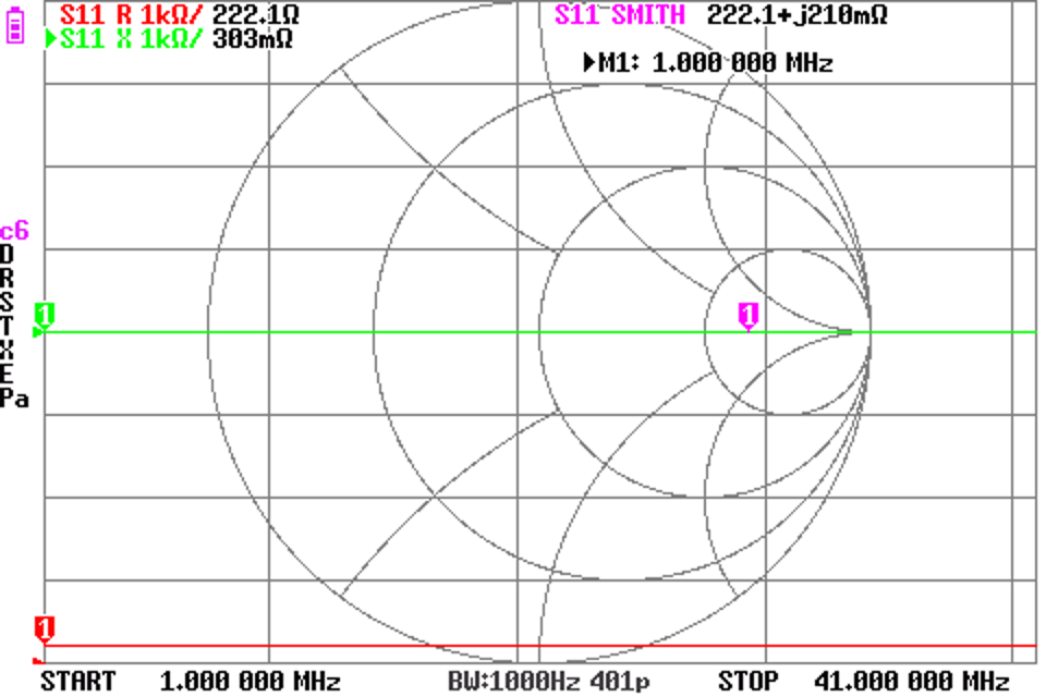
At a given frequency, we can say that \(\frac{\beta l}{Z_0} \propto \frac{t}{Z_0}\) and that \(t_{50} \equiv t_{Z_0}\frac{50}{Z_0}\) and since \(l \propto t \text{, } l_{50} \equiv l_{Z_0}\frac{50}{Z_0}\). These equivalences allow transforming a length or propagation time at actual Z0 into an equivalent length or time at Z0=50. For example if the propagation time of a fixture of 6mm length of air spaced line with Z0=200Ω was 20ps, an equivalent one way e-delay at Z0=50Ω (the instrument reference) of \(t_{50} =20\frac{50}{200}=5 \text{ ps}\) would approximately correct the transmission line effects of the 20ps of 200Ω line. Note that for an s11 correction, the two way e-delay is needed, 10ps in this example.

An important thing to remember is that port extension using e-delay assumes a lossless port extension using transmission line where phase length is proportional to f.

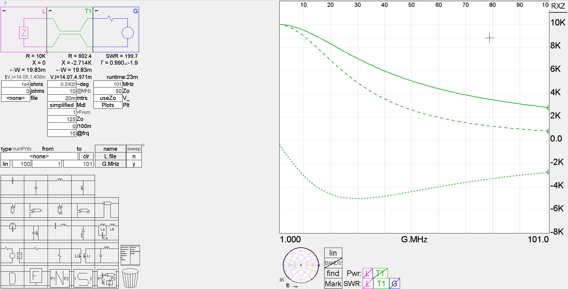
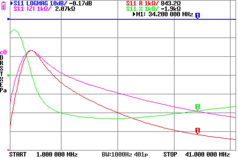
Above is a SimNEC simulation of Zl=10000+j0Ω with 0.025rad 200Ω lossless line backed out by -0.1rad of lossless 50Ω line (comparable to e-delay). The green reversal path lies almost exactly over the magenta path of the original transmission line transformation.

Summary for Zl>>Zo

\(Y_{in}=Y_l +\jmath \frac{\beta l}{Z_0}\\\) \(t_{50} =t_{Z_0}\frac{50}{Z_0}\\\) \(l_{50} =l_{Z_0}\frac{50}{Z_0}\)

Zl<<Zo

Recalling that the expression for Zin of a lossless transmission line terminated in Zl is:

\(Z_{in}=Z_0 \frac{Z_l+\jmath Z_0 tan(\beta l)}{Z_0+\jmath Z_l tan(\beta l)}\\\)

For \(Z_l \ll Z_0 \text{, } Z_l tan(\beta l) \ll Z_0\) and can be ignored.

\(Z_{in}=Z_0 \frac{Z_l+\jmath Z_0 tan(\beta l)}{Z_0}\\\) \(Z_{in}=Z_l+\jmath Z_0 tan(\beta l)\)

Where \(\beta l \lt 0.1\) applies:

For short electrical length, \(\beta l<0.1\), \(tan(\beta l) \approx \beta l\):

\(Z_{in}=Z_l+\jmath Z_0 \beta l\\\)

So, the effect of this transmission line is to add a small +ve (inductive) series reactance to Zl.

\(\beta l Z_0\) is interesting:

\(\beta l Z_0= \frac{2 \pi f Z_0}{c_0 v_f} t c_0 v_f=2 \pi f Z_0 t\\\)

Where \(\beta l\frac{Z_0}{50} \lt 0.1\) also applies:

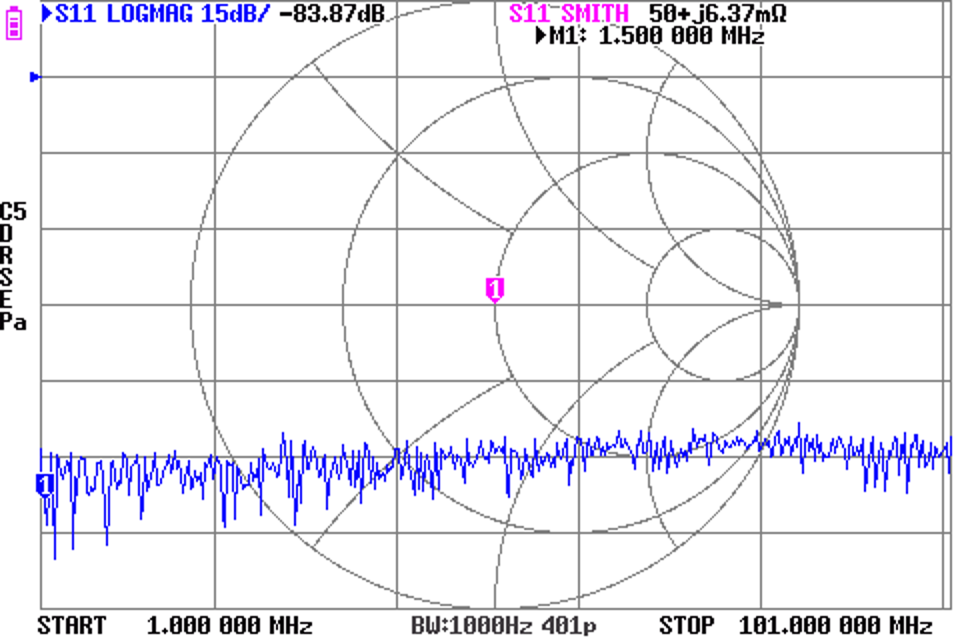
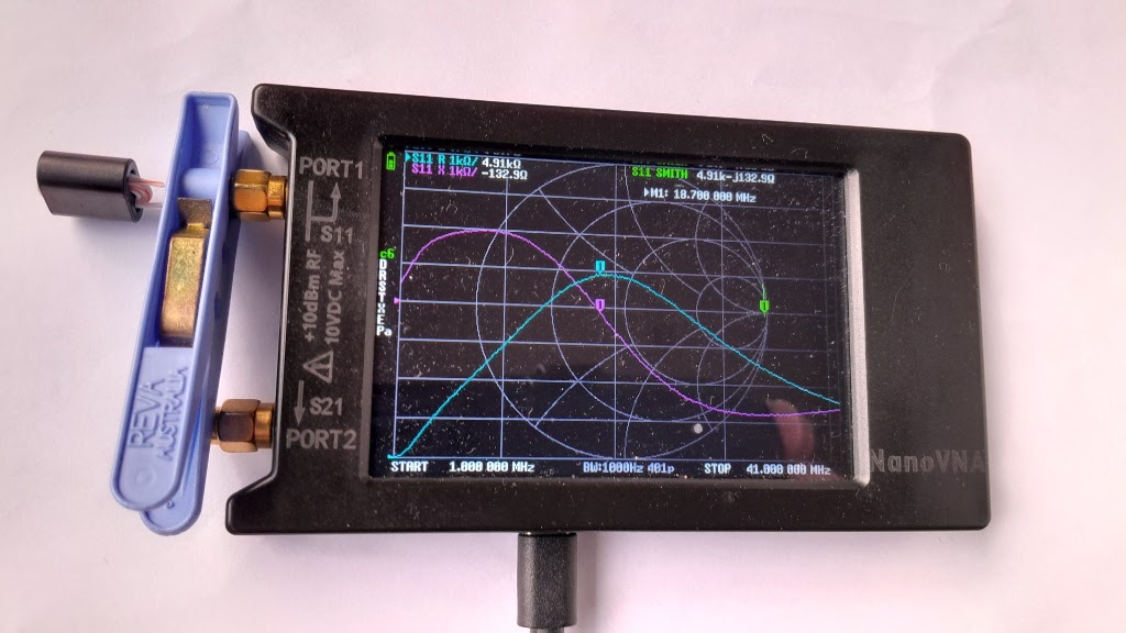
At a given frequency, we can say that \(\beta l Z_0 \propto t Z_0\) and that \(t_{50} \equiv t_{Z_0}\frac{Z_0}{50}\) and since \(l \propto t \text{, } l_{50} \equiv l_{Z_0}\frac{Z_0}{50}\). These equivalences allow transforming a length or propagation time at actual Z0 into an equivalent length or time at Z0=50. For example if the propagation time of a fixture of 6mm length of air spaced line with Z0=200Ω was 20ps, an equivalent one way e-delay at Z0=50Ω (the instrument reference) of \(t_{50} =20\frac{200}{50}=80 \text{ ps}\) would approximately correct the transmission line effects of the 20ps of 200Ω line. Note that for an s11 correction, the two way e-delay is needed, 160ps in this example.

An important thing to remember is that port extension using e-delay assumes a lossless port extension using transmission line where phase length is proportional to f.

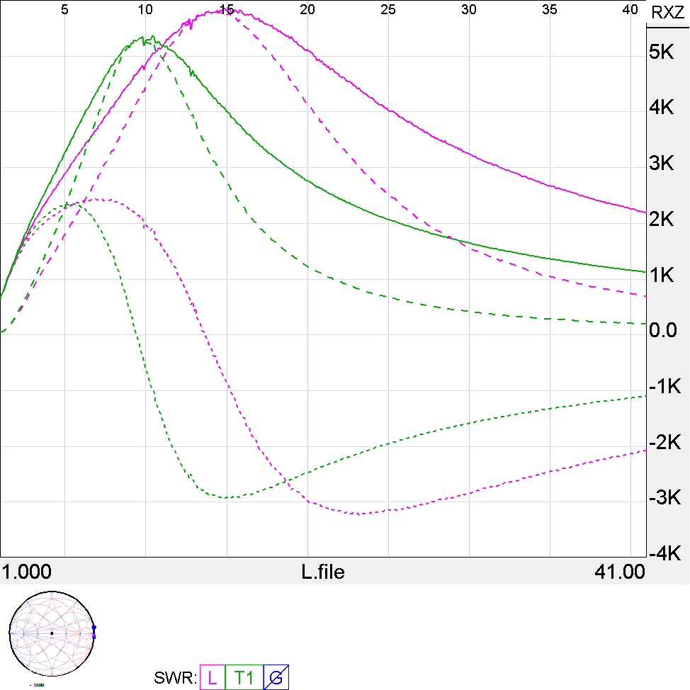
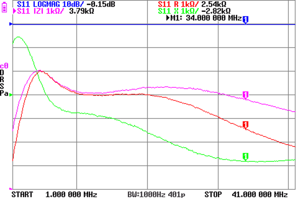
Above is a SimNEC simulation of Zl=1+j0Ω with 0.1rad lossless 200Ω line backed out by -0.025rad of lossless 50Ω line (comparable to e-delay). The green reversal path lies almost exactly over the magenta path of the original transmission line transformation.

Summary for Zl<<Zo

\(Z_{in}=Z_l+\jmath Z_0 \beta l\\\) \(t_{50} =t_{Z_0}\frac{Z_0}{50}\\\) \(l_{50} =l_{Z_0}\frac{Z_0}{50}\)


Last update: 9th August, 2024, 11:57 PM

nanoVNA-H – Deepelec test jig #2

By: Owen
17 July 2024 at 22:59

I have found you can never have enough of these things. It is very convenient to leave some measurement projects set up while work continues on some parallel projects.

Above is the kit as supplied (~$8 on Aliexpress). Note that it does not contain any male turned pin header… more on that later.

I was critical of Alixpress four years ago when I purchased the last one, but things have improved greatly in that time, to the point they are often faster delivery that eBay’s “Australian stock” sellers.

Carefully break off 7 x 7 way pieces of the turned pin female header and ‘dry’ fit them to the board, Now get two more pieces of header that are at least 7 way, and plug them at right angles to the ones already placed to set the spacing. Now solder them to the board (hint: liquid flux makes this job easier.) The ‘donuts’ are quite small, use a tip that gives contact to the donut so that heat is applied to the pin and the ‘tube’ for a good solder joint.

Test the coax connectors on a good male connector to be sure they are not defective… quality of these is poor. I tighten them to 0.8Nm to seat and form the female connector. If the threads bind, chuck them now rather than after you have soldered them in place.

I installed only the mid connectors on this board, I have another which has all the connectors and I have never used the other four. Carefully position and solder the connectors, again liquid flux helps.

The clear plinth does not come in the kit, it is my addition.

Above, the plinths designed in Freecad were cut out of 3mm clear PVC.

They are cut using a single flute 2mm carbide cutter.

You could easily make them with hand tools and a drill. M2.5×6 nylon screws are used to attach the plinth to the hex spacers (supplied), giving the assembly four non-scratch feet.

Now the kit is incomplete. You are going to need some parts you see above built on male turned pin header strip. The kit does contain some 49.9Ω resistors you can use for a LOAD, you will also need an OPEN (centre left) and a SHORT (lower right). Others are for connecting the sections of the test board and THROUGH calibration.

The SMA connector at left is another test fixture which uses the same calibration parts. It can be used directly on the NanoVNA or at the end of a convenient length of cable. I originally made it to use on a Rigexpert AA600, either on a N(M)-SMA(F) adapter, or a short N(M)-SMA(F) cable.

It is bit hard to see the connections on the board when it is populated, so I have made the graphic above, printed it and laminated it for handy reference.

Note that the connections are a little different to the SDR-Kits jig (that they probably copied), in particular C2, C6, E2 and E6 are each not connected to anything.

I have some custom made 300mm long RG400 cables that I use with these, labelled for calibration purposes. IIRC they cost about $30 per pair from RFSupplier.com.


Last update: 18th July, 2024, 9:20 AM

Common mode choke measurement – length matters #3

By: Owen
15 July 2024 at 21:06

Following on from Common mode choke measurement – length matters #2 which demonstrated that the following test fixture gave invalid results due to the 20mm length of resistor pigtails, the connection length in general terms

Above is a pic of my experimental setup. The resistor on Port 1 is a 10k 1% metal film resistor. The NanoVNA has been SOL calibrated at the Port 1 jack.

These plots should be horizontal lines at R=10k and X=0. They can be improved by shortening the connections, try the experiment yourself, you will learn more than if I show you the results.

If you do the experiment, you will be better placed to critically appraise the test configurations that abound online, especially on Youtube, and form a view as to whether the results are credible.

A thought exercise: do you think the fixture for this choke is good?


Last update: 16th July, 2024, 7:11 AM

Common mode choke measurement – length matters #2

By: Owen
11 July 2024 at 17:18

Following on from Common mode choke measurement – length matters

Lots of people have reported experiments to show gross failure of s11 reflection measurement of high impedances such as those encountered measuring common mode chokes.

Above is a chart of a “10k resistor with leads” from (G4AKE 2020), the curve of interest is the s11 curve which he describes as unsuitable. He did not publish enough information to critique his measurement… so I will conduct a similar experiment.

My experiment

Above is a pic of my experimental setup. The resistor on Port 1 is a 10k 1% metal film resistor. The NanoVNA has been SOL calibrated at the Port 1 jack.

Above is a screenshot of the measurement. Quite similar result to that shown in (G4AKE 2020). (Note R, X, s11 phase at the marker.)

Note the s11 phase plot, we see the phase of s11 falling at a uniform rate from 1 to 101MHz.

What should we expect?

s11 for a 10k+j0 DUT should be 0.990050+j0 or 0.990050∠0.000° independent of frequency.

But we see this linearly decreasing phase. It is a big hint, transmission lines do this sort of thing.

So what if we attempt an approximate correction using e-delay.

e-delay of 54.5ps flattens the phase response, and the R and X values are closer to ideal, not perfect, but much closer than the uncompensated plot earlier.

A SimNEC simulation

Above is a SimNEC simulation of my experiment.

Conclusions

  • An experiment to duplicate G4AKE’s measurement achieves similar response.
  • Drilling down on the detail of the experiment response hints that the resistor pigtails contribute transmission line effect that are the main cause of the poor response.
  • An approximate compensation of the transmission line effects gives an impedance measurement that is much better than G4AKE’s recommended s21 series through measurement.
  • G4AKE condemns s11 impedance measurement as unsuitable, but there is good reason his fixture was the main reason for poor results… length matters.
  • Read widely, question everything.

References

Mar 2020. G4AKE. Measuring high and low impedance at RF.

Last update: 12th July, 2024, 7:57 AM

Common mode choke measurement – length matters

By: Owen
11 July 2024 at 08:20

There must be thousands of Youtube videos of “how to measure a common mode choke” to give a picture of some sort of the test configuration… though most lack important detail… and detail IS important in this case. Likewise there are lots of web pages on the same subject, and some have pics of the test configuration, again mostly lacking important detail.

For the most part, these show test configurations or ‘fixtures’ that might be appropriate for audio frequencies, but are unsuitable at radio frequencies, even at HF.

Connecting wires at radio frequencies are rarely ideal, the introduce some impedance transformation that may or may not be significant to the measurement project at hand. Such connections can be thought of as transmission lines, often mismatched so they have standing waves (meaning the impedance of the load appears to vary along the line.

Let’s take the DUT in my recent article Baluns: you can learn by doing! as an example for discussion.

Let’s take the saved s1p file from a S11 reflection impedance measurement as the example.

Above is a plot of the common mode impedance of the choke, solid line is |Z|, dashed line is R, dotted line is X. This was measured with connecting wires <10mm, see the original article.

Now lets transform that to what we would see if just 100mm of 300Ω lossless line was used to connect the VNA to the balun.

The green curves are what would now be measured by the VNA. Observe the shift in the self resonant frequency (where X passes through zero), observe the shift in frequency of maximum |Z|, and the change in maximum |Z|.

These curves are like they were from different baluns.

Above is an example from a tutorial Youtube video by Fair-rite (a ferrite core manufacturer). Can you work out and draw a schematic of the test fixture? IIRC, the fixture itself was not calibrated, it cannot be because some of it is coax with the shield at one end disconnected.

A clear pic of the detail of all connections and how / where the fixture is calibrated is essential to interpreting any measurements.

A guide I often give people is this:

if you reduce the length of connections and measure a significant difference, then:

  • they were too long; and
  • they may still be too long.

Iterate until you cannot measure a significant difference.

Make some measurements with different fixture configurations, analyse the results and learn more about fixtures that you will glean from this or probably any written article or Youtube video.

If you believe s21 series through measurement technique or some other technique magically corrects poor fixtures, measure them and critically analyse the results… are they magic?

Read widely, question everything.

Last update: 11th July, 2024, 7:03 PM

Common mode choke measurement – estimating Cse

By: Owen
11 July 2024 at 04:26

The article Baluns: you can learn by doing! presented measurements of a Guanella 1:1 Balun, a common mode choke.

Above is the prototype balun being a Fair-rite 5943003801 (FT240-43) wound with 11t of solid core twisted pair stripped from a CAT5 solid core LAN cable and wound in Reisert cross over style. Note that Amidon #43 (National Magnetics Groups H material) is significantly different to Fair-rite #43.

Above is a plot of the R and X components of Zcm taken from the .s1p file saved during measurement.

Note that it exhibits a self resonance at 13.5MHz. It is not simply an inductor, it is a resonator with an observed self resonant frequency (SRF) of 13.5MHz.

We can predict the impedance of the choke at low frequencies using the complex permeability, core parameters and turns, but as frequency approaches SRF some adjustment needs to be made to accommodate the self resonance. A simple adjustment is to shunt the simple inductor with some value of equivalent capacitance Cse that would cause the simple inductor to resonate at the observed SRF. This measure improves prediction of impedance up to SRF and a little higher depending on your accuracy requirement.

Above is a prediction based on µ, turns etc at the SRF. You will note that the calculated impedance is not consistent with resonance, but it can be used to calculate the Cse that would resonate it.

See also Ferrite permeability interpolations.

You could discover that Cse by inputting a value for Cse and iteratively increasing / decreasing it to find the value where the X part of Z passes through zero… but it is very tedious. You could use a hand calculator to find the value of C with B=0.0001116S.

Or you could use Solve Cse for self resonant inductor.

Above is calculation directly of Cse from calculated R, X at SRF and SRF. Note that you cannot measure R, X of the simple inductor as a practical inductor has the inseparable effects of self resonance, it comes as a bundle.

You could then return to the first calculator and enter the calculated value for Cse and so calculate the expected choke impedance etc.

Above, calculation of the choke using the calculated Cse. The calculated values to not reconcile exactly with measurement, measurement has errors, but worse, ferrites have quite wide tolerances.

Read widely, question everything.

Last update: 11th July, 2024, 2:33 PM

NanoVNA examination of stacked ferrite cores of different mixes – more detail

By: Owen
26 June 2024 at 04:33

NanoVNA examination of stacked ferrite cores of different mixes studied an example stacked core scenario, presenting measurements of a stack of BN43-202 and BN73-202, 5t wound through both.


The article stated:

They are somewhat similar (but only somewhat) to two series chokes with the same number of turns, so you might expect overlap of the responses.

Above is the measurement of the stacked configuration.

This article compares the stack with measurement of two series chokes of the same number of turns.

Above is the measurement of the series configuration.

They appear quite similar up to perhaps 5MHz or so, lets compare R, X on the same graph.

The magenta and cyan traces are R and X for the stacked configuration.

Below self resonance peaks, they are very similar which hints that the stacked cores are approximately the sum of responses of each of the cores at lowish frequencies, but as resonance comes into play, they differ.

It is clear that the stacked cores do not behave as equivalent chokes in parallel, that proposition is very wooly thinking.

This is measurement of a specific scenario, and the results cannot simply be extended to other scenarios. I have not (yet) been able to create a simple model of the stacked cores above self resonance, I would suggest that for reliability, any proposed configurations be measured. Whilst in this case, the series configuration appears to have a better impedance characteristic, that might not apply to other geometries and mixes.

Build, measure, learn.

Read widely, question everything.

Last update: 28th June, 2024, 8:48 AM

Effective measurement of common mode current on a two wire line – a user experience

By: Owen
23 June 2024 at 15:05

This article reports and analyses a user experiment measuring current in a problem antenna system two wire transmission line.

A common objective with two wire RF transmission lines is current balance, which means at any point along the transmission line, the current in one wire is exactly equal in magnitude and opposite in phase of that in the other wire.

Note that common mode current on feed lines is almost always a standing wave, and differential mode current on two wire feed lines is often a standing wave. Measurements at a single point might not give a complete picture, especially if taken near a minimum for either component.

MFJ-854

The correspondent had measured feed line currents using a MFJ-854.

Above is the MFJ-854. It is a calibrated clamp RF ammeter. The manual does not describe or even mention its application for measuring common mode current.

So, my correspondent had measured the current in each wire of a two wire transmission line, recording 1.50 and 1.51A. He formed the view that since the currents were almost equal, the line was well balanced.

I have not used one of these, I rely on my correspondents guided measurements. (I have used the instrument described at Measuring common mode current extensively.)

MFJ-835

This is the instrument that MFJ sell for showing transmission line balance. One often sees recommendations by owners on social media, it is quite popular.


If the needles cross within the vertical BalancedBarTM the balance is within 10%. If not, you know which line is unbalanced and by how much.

Note the quote uses current like it is a DC current, not an AC current with magnitude and phase.

So, in the scenario mentioned earlier, the needles would deflect to 50% and 50.3% on the 3A scale, the needles would cross right in the middle of the BalancedBarTM, excellent.

… or is it?

One more measurement with the MFJ-854

I asked the chap to not only measure the (magnitude) of the current in each wire, but to pinch the wires together and close the clamp around both and measure the current. The remeasured currents were of 1.50 and 1.51A in each of the two wires, the current in both wires bundled together was 1.2A.

What does this mean?

With a bit of high school maths using the Law of Cosines, we can resolve the three measured currents into common mode and differential mode components.

Above is the result, the current in each wire comprises a differential component of 1.38A and a common mode component of 0.6A. The common mode components in each wire are additive, so the total common mode current on the feed line is 1.2A.

Above is a phasor diagram of I1, I2 and I12, and the components Ic and Id.

Note in this diagram that whilst the magnitude of i1 and i2 are similar, they are not 180° out of phase and that gives rise to the relatively large sum I12 (the total common mode component of I1 and I2).

This is a severe imbalance, sufficient to indicate a significant problem and to prompt a physical and electrical check of the antenna and feed line conductors and insulators.

Repairs were made and the measured result was quite good.

Above are the measurements and calcs.

Above is the phasor diagram… a bit harder to read as there is very little common mode current.

By contrast with the previous case I1 and I2 are almost 180° out of phase and the sum of them, I12 has very small magnitude.

Conclusions

The MFJ-854 can be used effectively for measuring current balance.

Understanding the relative common mode and differential components hinted there was something very wrong in the antenna system.

Forget the MFJ-835 for proving balance. If the needles do not cross in the BalancedBarTM it indicates unbalanced amplitudes. If they do cross in the BalancedBarTM it indicates approximately balanced amplitude, but does not prove the phase relationship is approximately opposite and as shown in this example, is a quite erroneous result.

Last update: 24th June, 2024, 9:00 AM

Dislord’s NanoVNA-D firmware v1.2.35 includes a facility to apply a correction based on the DC resistance of the LOAD

By: Owen
22 June 2024 at 21:56

A recent series of articles discussed the question of how accurate does a calibration LOAD need to be.

Following on from that I requested a change to allow the actual resistance of LOAD to be used

These tests are not conducted in a temperature stable laboratory, so allow some latitude in results.

The NanoVNA-H running NanoVNA-D firmware v1.2.35 was SOL calibrated, but the calibration kit had a LOAD that measured 51.273Ω at DC using a high accuracy ohmmeter.

Above is an |s11| sweep after calibration. Measurement is limited by the instrument noise floor, about -80dB @ 1MHz. This says nothing about the load as it is based on a flawed calibration, but it shows us the noise floor. For reasonable accuracy, we might say here that we can measure |s11| down to about -70dB… subject to an accurate calibration LOAD.

Now that LOAD sets the instrument’s calibration reference impedance to 51.273Ω and if I was to measure a true 50Ω DUT, we would expect |s11|=-38dB.

I do not have a termination that is exactly 50Ω, so let’s measure another termination that measured 49.805 at DC using a high accuracy ohmmeter. We would expect the VNA based on the calibration above to show|s11|=-36.8dB.

Above is a screenshot of exactly that measurement, calibrated with 51.273Ω and measuring 49.805Ω, expect |s11|=-36.8dB and we get -36.6dB. That reconciles well.

Now lets specify the “Standard LOAD R”.

Above is a screenshot of the data entry.

Now with the correction applied, let’s measure the termination that measured 49.805 at DC using a high accuracy ohmmeter. We would expect the VNA to now show|s11|=-54.2dB.

Above is a screenshot of exactly that measurement, calibrated with 51.273Ω, “Standard LOAD R” correction applied for that value, and measuring 49.805Ω, expect |s11|=-54.2dB and we get -53.1dB. That reconciles well.

So what is the effective directivity with the “Standard LOAD R” correction?

If the measurement of the LOAD was without error, then the limit for low jitter measurement would be around 10dB above the noise floor measured earlier, so say |s11|=-70dB, which corresponds to ReturnLoss=70dB.

You could use that ReturnLoss as coupler Directivty in Calculate uncertainty of ReturnLoss and VSWR given coupler directivity to calculate uncertainty of a given measurement.

Above is a sample calculation.

But, measurement of LOAD has uncertainty.

Let’s say you measure LOAD with 1% uncertainty, and you measure 49.0Ω , but it could be as low as 48.5Ω (ie -1%), we can calculate the implied inherent ReturnLoss of the 48.5Ω using Calculate VSWR and Return Loss from Zload (or Yload or S11) and Zo) .

The LOAD could be specified as 48.5Ω with ReturnLoss=45dB.

So, entering “Standard LOAD R” is better than using the default 50Ω, but due to the uncertainty of measurement of that LOAD, the instrument Directivity is around 45dB. So, you can see that the accuracy of measurement of LOAD flows into the effective instrument Directivity which feeds calculation of s11 measurement uncertainty.

The instrument I used to measure the terminations has uncertainty of 0.035Ω on a 50Ω reading, which corresponds to a ReturnLoss of 69dB.

By contrast for example, a Fluke 106 has specified uncertainty of 1.1% at 50Ω which implies ReturnLoss 45dB… you are probably better just accepting 50Ω unless you know the LOAD is really bad.

SDR-kits sells relatively inexpensive calibration kits where they supply the measured DC resistance of LOAD.

Last update: 23rd June, 2024, 11:24 AM

NanoVNA examination of stacked ferrite cores of different mixes

By: Owen
22 June 2024 at 08:19

A chap asked the assembled experts online:

Has anybody tried stacking say a type 43 on top of a 61 on top of a 31 for a wider bandwidth? Would the losses be any greater than using one toroid for each band?

There were some very firm assertions that this will not work well (without evidential support of course). Beware of firm assertions!

Quickly the case was compared to parallel chokes… and there is no parallel (pardon the pun), they are not the same.

They are somewhat similar (but only somewhat) to two series chokes with the same number of turns, so you might expect overlap of the responses. Two series chokes carry the same current and with the same number of turns apply the same magnetomotive force (mmf) to both magnetic cores.

But rather than hypothesise, even if from experience… lets measure.

Above is the DUT. It is a stack of BN43-202 and BN73-202, 5t wound through both. This is not two chokes in series, it is just like stacking a FT240-43 and FT240-73 in concept.

Above is the measured choke impedance from 1-41MHz.

It has an impedance profile that is the sum of the contribution of both cores, it is not a low impedance result. |Z|>2kΩ from 1-34MHz.

I will leave it to readers to measure 5t on each core type and compare them.

But fact does not often get in the way of energetic discussions on social media. Do we know what fact (or truth) is anymore?

I will do some thinking here…

One of the concerns was this will increase heat loss and reduce the power handling of the combination.

My analysis is that loss in ferrite is related to the flux, which is related to the current. Deployed in an antenna system, the combination has higher impedance which will often lead to lower current, reducing flux and heating.

I would argue that appropriate combinations of core mixes is capable of a broader band higher impedance profile, and improved power handling.

Build, measure, learn.

Read widely, question everything.

NanoVNA examination of stacked ferrite cores of different mixes – more detail


Last update: 28th June, 2024, 2:00 AM

NanoVNA measurement of a coaxial filter

By: Owen
22 June 2024 at 06:03

This article discusses measurement of a coaxial filter. These are often referred to as “cavity filters”, but strictly speaking, a resonant cavity is different, these are a low loss transmission line section without input and output coupling.

The DUT is a single coaxial resonator configured as a band pass filter with adjustable separate coupling loops. The inside of this nearly quarter wave tube is a coaxial rod grounded at the right had end and almost reaching the left hand end with coupling loops attached to the coax connectors. The rod length is adjustable to tune it, everything is silver plated brass. The adjustable coupling loops allow some adjustment of bandwidth, but narrow bandwidth brings higher loss.

The filter is currently set for its tightest coupling, widest bandwidth, lowest loss.

It was last used for experiments to show that some ham grade receivers commonly used lack sufficient front end selectivity to deliver in the real world, the ‘shielded room’ performance stated in the specifications.

The instrument used here is a NanoVNA-H4 v4.3 and NanoVNA-D firmware NanoVNA.H4.v1.2.33.

It was SOLIT calibrated at the ends of 300mm RG400 patch leads on both ports. It was attached to the DUT with SMA(F)-N(M) adapters.

Let’s assess the NanoVNA s21 noise floor

Above is a plot of the noise in the s21 path, the noise floor is approximately -80dB, so measurements cannot be made with confidence down to about -70dB.

Whilst that noise floor probably permits measuring single stage rejection, especially with notches in duplexer filters, it is probably not sufficient to measure a cascade of two filter sections, much less three (which is a common configuration).

Now the measurement of s11 and s21

Above is a wide sweep from 130-160MHz (note the changed |s21| scale from the previous screenshot.

Above is a narrower sweep  over the ~3dB bandwidth. 3dB bandwidth is about 800kHz. ReturnLoss>20dB bandwidth (VSWR<1.2) is less than 100kHz (ReturnLoss=-|s11|.)

What if it had a notch filter as well?

We might expect that a notch would be 30dB to more than 50dB down. That is far enough above the |s21| noise floor to measure, but the notch of a cascade of filter sections will probably dip into the noise.

It might seem sufficient to measure the depth of notch in one stage of a filter, but thorough measurement requires assessment of the notch overall to demonstrate that they all line up on the correct frequency.

So, the often asked question…

Is this NanoVNA suitable for alignment and measuring performance of a typical repeater duplexer?

IMHO, no, it lacks sufficient dynamic range to measure the notch depths typically required.

Last update: 22nd June, 2024, 4:04 PM

Common mode choke measurement – for beginners

By: Owen
20 June 2024 at 22:53

I have corresponded with many people trying to make valid measurements of a Guanella 1:1 balun, also known as a common mode choke.

In common mode, the device looks like a ferrite cored inductor. That might sound simple, but it is anything but, and it can be a challenge to measure.

There are lots of measures quoted, most of them IMHO are bogus or incomplete, usually specious… which accounts for their popularity.

This article focusses on making a valid measurement of the R and X components of the choke’s common mode impedance by the simplest means that is likely to give direct results.

Let’s start by proving the measurement instrument

I have taken an ordinary 1% metal film resistor and measured it with an accurate ohmmeter to be 221.4Ω. That is good, it reconciles with its markings. Now this is not a pure resistance at RF, it has some self inductance so we must expect to see that when measured with the VNA.

The wires are trimmed short. The bare end can be safely inserted into the centre pin of a SMA(F) jack.

One wire is poked into the Port 1 centre pin and the plastic clothes peg secures the other wire to the outside male threads of the SMA jack. Alternatively you could use a zip tie to secure the other wire to the outside male threads of the SMA jack.

Above, the test configuration.

Above, a screenshot. Focusing on the marker at 1MHz so that self inductance effects are small, we measure Z=222.1+j0.303. That reconciles well.

Now let’s move on to an unknown inductor

To simulate a small common mode choke, I have wound a Fair-rite 2843000202 (BN43-202) binocular core with 6t of single conductor stripped from an 4pr LAN cable. Note the specific core part, non-genuine parts may have different responses. The wires are trimmed short and 8mm of insulation stripped.

The bare end can be safely inserted into the centre pin of a SMA(F) jack.

Above is the test setup. One wire is poked into the Port 1 centre pin and the plastic clothes peg secures the other wire to the outside male threads of the SMA jack. Alternatively you could use a zip tie to secure the other wire to the outside male threads of the SMA jack.

The key thing is very short connections, they are less than 0.6° over the frequency range measured.

Here is a screenshot. The inductor is self resonant around 18.7MHz. The R and X curves are very similar to what you would get for a practical Guanella 1:1 balun though commonly the resonance would be somewhat lower, below 10MHz often. Narrower peaks will be observed with lower loss ferrite, eg #61 mix.

For the enquiring mind

If you have your own technique, fixture, test jig, cables etc try measuring a resistor like this and a choke like this (preferably exactly like this) by the method I have shown and your own technique and compare them.

Read widely, question everything.

Last update: 21st June, 2024, 8:53 AM

NanoVNA – how accurate does the LOAD need to be – part 3?

By: Owen
19 June 2024 at 23:20

NanoVNA – how accurate does the LOAD need to be – part 2? answered the question in the context of an instrument that assumes the LOAD is exactly 50+j0Ω.

As mentioned in the article, there are more sophisticated models of the imperfection of nominal SHORT, OPEN and LOAD calibration parts (or ‘standards’), but the NanoVNA-H4 does not currently implement any of them.

A simple improvement is to accurately measure the DC resistance of the LOAD part, and use that resistance to calculate the expected LOAD response, and to use that in calculating the error terms that will be used in correction of raw measurements.

Precision Loads are expensive

LOADs with specified high ReturnLoss is an expensive option. Try to find a LOAD with ReturnLoss>40dB (VSWR<1.02)  for less than the price of the entire NanoVNA.

Roll your own

Another option is to buy some 0.1% 100Ω SMD resistors (50 for $7 on Aliexpress) and make a LOAD device that is suitable for calibration, but it is challenging to make such a lot that is good above say 100MHz.

Select for DC resistance

An option I have used is to buy a few inexpensive 6GHz Chinese terminations (~$6 ea) and measure their DC resistance, selecting the best as ‘good’ terminations. The best of a bunch of three I purchased had Rcd=49.085 which equates to RL50=54dB.

If the NanoVNA-H4 supported calibration based on DC resistance of the LOAD…

Some suppliers offer inexpensive calibration kits with measured DC resistance, eg SDR-KITS.

Some users may have a 4W ohmmeter that is capable of high accuracy measurement of loads, preferably to 0.1% uncertainty or better.

If the DC resistance was used during calibration / correction, then the instrument Directivity at frequencies below about 100MHz would be limited mainly by the instrument noise floor.

I have suggested such a facility to Dislord for NanoVNA-D so that its accuracy as a stand alone VNA can be improved.

See Dislord’s NanoVNA-D firmware v 1.2.35 includes a facility to apply a correction based on the DC resistance of the LOAD for implementation details.


Last update: 23rd June, 2024, 7:57 AM

NanoVNA – how accurate does the LOAD need to be – part 2?

By: Owen
19 June 2024 at 09:26

This article continues on from NanoVNA – how accurate does the LOAD need to be – part 1?

Measures such as ReturnLoss, Gamma, s11, ro |s11|, VSWR are all wrt some reference impedance, often, but not necessarily 50+j0Ω.

The process of SOL calibration of a VNA, and its subsequent correction of DUT measurements, means that raw measurements are corrected with error terms that are derived from the calibration measurements and a set of responses expected of the calibration parts.

Those responses may be ideal responses; a simple short circuit (sc), a simple open circuit (oc) and an ideal load of some nominal value (say 50+j0Ω).

More sophisticated calibration may use a more accurate model for each of the SOL components, but NanoVNA uses simple ideal models for the SOL parts, including that L is 50+j0Ω.

So, if you use for example a 55Ω resistor for LOAD, then the correction factors are calculated to correct the raw measurement for a 55+j0Ω DUT to have \(s_{11}= \frac1{\infty}+\jmath 0\) (though noise will result is a lesser value, perhaps around 1e-40), and it its further computation assumes that s11 is wrt 50Ω, so it will render that DUT impedance as 50+j0Ω, ReturnLoss in dB as a very large number (perhaps 80dB).

If you did connect a DUT that was exactly 50+j0Ω, it will ‘correct’ the raw measurement to s11=-0.04762+j0, and it will render that DUT impedance as 45.45+j0Ω, ReturnLoss in dB as 26.4dB.

Saying it renders ReturnLoss as 26.4dB for an ideal 50+j0Ω DUT is equivalent to saying it has a Directivity (wrt 50Ω) of 26.4dB.

We can return to Calculate uncertainty of ReturnLoss and VSWR given coupler directivity and calculate the uncertainty of that system when it indicates for an unknown DUT, a ReturnLoss of say 21dB (equivalent to VSWR=1.2).

So for DUT with displayed ReturnLoss=21dB, actual ReturnLoss wrt 50Ω could be anywhere from 17.3dB to 27.7dB… quite a range!

So, to obtain a reasonably low uncertainty range, the Directivity of the instrument (the ReturnLoss of the LOAD calibration part) needs to be perhaps 10dB better than the DUT… use the calculator to try different instrument Directivity values and DUT measured ReturnLoss to find a combination with acceptable uncertainty.

So if you did want to measure ReturnLoss with uncertainty of less than 3dB, you might find the following works.

So, minimum coupler directivity is 32dB, you will need a LOAD calibration part that has ReturnLoss>32dB, equivalent to VSWR<1.05. That is a pretty practical component, and will not be outrageously expensive.

An exercise for the reader: what LOAD part ReturnLoss is needed to measure ReturnLoss of 30dB (VSWR=1.065) with less than 3dB uncertainty.

So, whilst you might see |s11| displays on your NanoVNA showing -30dB, they have very wide uncertainty unless the L calibration part is one of high accuracy.

Last update: 20th June, 2024, 9:21 AM

Verify coax cable performance with NanoVNA

By: Owen
18 June 2024 at 23:45

This article walks through a simple verification of nominal 50Ω coax cable with connectors against manufacturer specifications using a NanoVNA.

The instrument used here is a NanoVNA-H4 v4.3 and NanoVNA-D firmware NanoVNA.H4.v1.2.33.

The DUT is a 10m length of budget RG58-A/U coax with crimped Kings BNC connectors, budget but reasonable quality. It was purchased around 1990 in the hey day of Thin Ethernet, and at a cost of around 10% of  Belden 8259, it was good value.

The notable thing is it has less braid coverage than 8259 which measures around 95%.

The cable has BNC(M) connectors, and BNC(F)-UHF(M) + UHF(F)-SMA(M) are used at both ends to simulate the impedance transformation typical of a cable with UHF(M) connectors.

Step 1: calibrate and verify the VNA

Note that |s11|<-40dB, or ReturnLoss>40dB. You really want at least 30dB ReturnLoss for this test to be as simple as described here.

The Smith chart plot of s11 is a very small spiral in the centre of the chart… approaching a dot.

Step 2: measure

The measurement fixture removed a ~150mm patch cable used during through calibration, so 750ps e-delay is configured on Port 2 to replace it. (one could just leave that cable in the test path and no e-delay compensation is needed).

Note that recent NanoVNA-D allows specification of e-delay separately for each port, don’t do as I have done if you use other firmware, leave the through calibration cable in place.

Above is a screenshot of the measurement from 1-31MHz.

Step 3: analysis

|s11|

Before rushing to the |s21| curve, let’s look at s11.

The Smith plot shows a small fuzzy spiral right in close to the chart centre, that is good.

The |s11| curve shows a periodic wave shape, lower than about -25dB. Recalling that ReturnLoss=‑|s11|, we can say ReturnLoss is greater than about 25dB. That is ok given the use of UHF connectors.

That wavy shape is mainly due to small reflections at the discontinuity due to the UHF connectors. They typically look like about 30mm of VF=0.67 transmission line of Zo=30Ω, so they create a small reflection. At some frequencies, the reflection from the far end discontinuity arrives in opposite phase with the near end reflection and they almost cancel, at other frequencies they almost fully reinforce, and in between they are well, in between… and you get the response shown in the screenshot. The longer the DUT, the closer the minima and maxima, and if the DUT is less than 180° electrical length, you will not see a fully developed pattern.

If you see a Smith chart spiral that is large and / or not centred on the chart centre, the cause could be that Zo of the DUT is not all that close to 50Ω, a low grade cable, possibly with migration of centre conductor or bunching of loose weave braid.

If your |s11| plot shows higher values, investigate them before considering the |s21| measurement. Check connectors are clean and properly mated / tightened.

|s21|

Now if that is all good, we can proceed to |s21|.

We can calculate InsertionLoss=‑|s21|, see Measurement of various loss quantities with a VNA.

It is interesting to decompose InsertionLoss into its components, because we may be more interested in the (Transmission) Loss component, the one responsible for conversion of RF energy to heat.

InsertionLoss for commercial coax cables is often specified as frequency dependent Matched Line Loss (MLL) or Attenuation (measured with a matched termination).

If InsertionLoss and MismatchLoss are expressed in dB, we can calculate \(Loss_{dB}=InsertionLoss_{dB}-MismatchLoss_{dB}\)

Above is a chart showing MismatchLoss vs ReturnLoss.  If ReturnLoss>20dB, MismatchLoss<0.05dB and can often be considered insignificant, ie ignored.

For example, the marker, ReturnLoss=26.05dB, so MismatchLoss is very small and can be ignored in this example and we can take that Loss≅InsertionLoss=‑|s21|.

We can calculate the MismatchLoss given |s11|:

As stated, at 0.011dB, it is much less than InsertionLoss so can be ignored.

So do we give this budget cable and connectors a pass?

At 15MHz, we can take MatchedLineLoss to be 6.8dB/100m which is a little higher than Belden 8259 datasheet’s 6.2dB/100m. That is not sufficient reason to FAIL the cable, we will give it a PASS.

Problem analysis

Let’s discuss a problem scenario to encourage some thinking.

Above is a through measurement after calibration.

What is wrong, shouldn’t |s11| be much smaller, shouldn’t the Smith chart plot be a dot in the centre?

Yes, they should.

If the calibration process was done completely and correctly, then this indicates that Zin of Port 2 is significantly different to the LOAD used for calibration. Note that they could BOTH be wrong. An approach to resolving this is to validate the LOAD, and when that is proven sufficiently accurate, remeasure Port 2 using a short through cable and check |s11|. If it is bad then perhaps a GOOD 10dB attenuator on Port 2 might improve things.

Now let’s ignore that problem and proceed to try the cable measurement (with that setup).

Above is a through measurement of an unknown 10m coax cable with 50Ω through connectors… no UHF connector issues here.

As before, look at |s11| first. The cyclic wavy nature hints that there is problem with one or more of LOAD, Port 2 Zin and DUT Zo. They should all be the same.

Note also the spiral Smith chart trace, if it is not centred on the centre of the chart, it hints that DUT Zo, LOAD and Port 2 Zin are significantly different.

So, to resolve this, one path is to validate the LOAD, and when that is proven sufficiently accurate, remeasure Port 2 using a short through cable and check |s11|. If it is bad then perhaps a GOOD 10dB attenuator on Port 2 might improve things. If these are both good, then the measurement suggests the DUT cable Zo is wrong.

The |s21| measurement is suspect until you resolve these issues.

Conclusions

Analysis of the |s11| measurement is important, good |s11| results are a prerequisite to analysing |s21|.

Comparison with manufacturers data gives a basis for PASS/FAIL.

Last update: 19th June, 2024, 3:08 PM

NanoVNA-h4 v4.3 Port 1 waveform

By: Owen
16 June 2024 at 22:51

This article documents the Port 1 waveform of my NanoVNA-h4 v4.3 which uses a MS5351M (Chinese competitor to the Si5351A) clock generator.

There are many variants of the NanoVNA ‘v1’, and most use a Si5351A or more recently a loose clone, and they will probably have similar output.

Above is the Port 1 waveform with 50+j0Ω load (power setting 0). By eye, it is about 3.3 divisions in the middle of each ‘pulse’. At 50mv/div, that is 165mVpp, 0.136W, -8.7dBm. The fundamental component (which is what is used for measurement below ~300MHz) is 3dB less, -11.7dBm.

Importantly, is is not a sine wave, it is a complex wave shape that is rich in harmonics. See square wave for more discussion.

Above is the Port 1 waveform with no load. By eye, it is about 6.6 divisions in the middle of each ‘pulse’. At 50mv/div, that is 330mVpp.

The voltage measurements are low precision, but suggest that if it behaves as a Thevenin source, since loaded voltage is half unloaded voltage, assuming that then Zsource=Zload=50+j0Ω.

How can you make good measurements with a square wave?

The instrument is mostly used to measure devices with frequency variable response, so how does that work (well)?

The NanoVNA-H is essentially a superheterodyne receiver that mixes the wave (send and received) with a local oscillator (LO) to obtain an intermediate frequency in the low kHz range, and digital filtering implements a bandpass response to reject the image response and reduce noise. So, whilst the transmitted wave is not a pure sine wave, indeed is rich in harmonics, the receiver is narrowband and selects the fundamental or harmonic of interest. The fundamental is used below about 300MHz, then the third harmonic is selected by the choice of the LO frequency above that, and still higher the fifth harmonic is selected.

Of course the power in the harmonics falls with increasing n which reduces the dynamic range of the instrument in harmonic modes. Though the NanoVNA adjusts power for the harmonic bands, one can observed a reduction in dynamic range.

How did you get those waveforms when it sweeps?

There is a stimulus mode labelled CW which causes output to be on a single frequency. In the sense that CW means continuous wave, and unmodulated sine wave, this is not CW but simply a single frequency approximately square wave. If you dial up 600MHz, the output is the fundamental 200MHz approximately square wave.

That is of little consequence if you use the NanoVNA’s receiver as a selective receiver, but if you use a broadband detector or power meter (which responds to the fundamental plus harmonic content), you may get quite misleading results.

The NanoVNA is not a good substitute for a traditional sweep generator that produced levelled sine waves of calibrated amplitude and had a source impedance close to 50+j0Ω

Last update: 18th June, 2024, 12:10 AM

Review of after market DeWalt compatible 18V 7Ah lithium-ion tool battery

By: Owen
16 June 2024 at 21:00

I purchased on of these batteries on Big-W online for a mid-high price ($77), expensive enough compared to genuine to expect it would have near to rated capacity.

Above is a pic of the battery advertised. The delivered battery was labelled 7Ah.

They say a picture is worth a thousand words:

So, there it is, after three charge discharge cycles to develop full capacity, two measured discharge cycles. It measures <2Ah, <30% of rated capacity.

Full refund claimed, promptly processed by Big-W Online – return label within a few hours.

Last update: 17th June, 2024, 7:00 AM

VNWA-3E – a ferrite cored test inductor impedance measurement – s11 reflection vs s21 series vs s21 pi

By: Owen
16 June 2024 at 04:51

This article is a remeasure of NanoVNA-H4 – a ferrite cored test inductor impedance measurement – s11 reflection vs s21 series vs s21 pi using a VNWA-3E of both a good and sub-optimal test fixture estimating common mode choke impedance by three different measurement techniques:

  • s11 shunt (or reflection);
  • s21 series through
  • s21 series pi;

Citing numerous HP (and successor) references, hams tend to favor the more complicated s21 series techniques even though the instruments they are using may be subject to uncorrected Port 1 and Port 2 mismatch errors. “If it is more complicated, it just has to be better!”

s21 series pi is popularly know as the “y21 method” (The Y21 Method of Measuring Common-Mode Impedance), but series pi better describes the assumed DUT topology.

What is an inductor?

Above is the test inductor, enamelled wire on an acrylic tube, an air cored solenoid.

We speak naively of this sort of component as an inductor, perhaps thinking it is a frequency independent inductance with perhaps some small series resistance. Let me make the distinction, Inductance is a property, Inductor is a practical thing (that includes Inductance… that might be a function of some variables).

Above is an s11 reflection measurement of the impedance of the air cored solenoid.

Above, focusing below about 5MHz, R is very low and X is approximately proportional to frequency, and the calculated equivalent series L is approximately independent of frequency… so the naive model discussed earlier might be adequate. Measured inductance at 1kHz is 20µH, at 5MHz apparent series inductance is still close to 20µH, but then starts rising, more quickly as the first resonance is approached (see previous plot).

We can calculate a value of shunt C that will resonate the inductor at this first resonance, in this case it is 1.02pF (often referred to as Cse). The parallel combination of 20µH and 1.02pF will have an impedance that is a good approximation of what was measured up to perhaps 1.2 times the frequency of the first resonance, BUT NOT ABOVE THAT. Such an equivalent circuit is useful, be be mindful of the acceptable frequency range.

The existence of higher order resonances shows that this is not simply an inductance. Calculated Cse will not explain the impedance curve much above the first resonance, it will NOT explain higher order resonances.

Understand the nature of the DUT

The DUT is a small test inductor, 6t on a Fair-rite 2843000202 binocular core (BN43-202).

We speak naively of this sort of component as an inductor, perhaps thinking it is a frequency independent inductance with perhaps some small series resistance.

You might look up the Al parameter for the core and calculate its inductance to be \(L=A_l n^2=2200*36=79,200 \text{ nH}\) and calculate its impedance @ 10MHz \(Z=\jmath 2 \pi f L=\jmath 2 \pi \text{ 1e7} \text{ 79.2e-6}=\jmath 4976\).

In fact it measures 3206+j1904, so the notion of a fixed inductance with small series resistance is not an adequate model for this component at HF. It exibits a first resonance at about 16.3MhHz.

In fact the DUT is a resonator, plotted here around its first resonance.

Using a ferrite core that is both lossy and frequency dependent permeability might make higher order resonances harder to observe, they are not simply harmonically related and they may be severely damped.

The test fixture

The test uses a small test inductor, 6t on a Fair-rite 2843000202 binocular core (BN43-202) and a small test board, everything designed to minimise parasitics. This inductor has quite similar common mode impedance to a HF good antenna common mode chokes.

Above is the SDR-KITS VNWA testboard.

The nanoVNA-H4 v4.3 was calibrated using the test board and its associated OSL components. The calibration / correction corrects Port 1 and Port 2 mismatch error. The test board is used without any additional attenuators, it is directly connected to the nanoVNA-H using 300mm RG400 fly leads.

Above, the test inductor mounted in the s11 shunt measurement position.

Above is the sub-optimal test setup, the DUT is connected by the green and white wires, each 100mm long.

Measurements and interpretation

Optimal

Above are the results of the three impedance measurement techniques.

Note that s21 series through and s21 series pi show no significant difference.

There is a difference between the s11 shunt method and the s21 series methods, the self resonant frequency is slightly different.

Sub-optimal

It is often held that the series pi or Y21 method corrects a sub-optimal fixture, but if you look closely, the series through and series pi curves have no significant difference between them, and they are only a little different to the plots from the optimal fixture… probably insignificant difference.

Does that mean series through undoes untidy fixtures in general? I doubt it.

Why the difference?

There are differences between the measurement methods, well between s11 shunt and s21 series through though in this case no significant difference from s21 series through to s21 series pi; and differences between the test jigs.

Note the test jig affected one measurement method differently to the other.

The results are sensitive to small changes in fixture layout, temperature, component tolerances etc

Sensitivity to parasitic fixture capacitance

Above is a chart of the measured s11 shunt impedance and two calculated values with 0.2pF of shunt capacitance subtracted and added. Note the effect on maximum R, and the self resonant frequency (SRF) (where X passes through zero).

From this information, we can calculate that the inductor at resonance is represented by some inductance with some series resistance, and Cse=1.5pF. So it is very easy for untidy fixtures, long connections etc to disturb the thing being measured.

BTW, for this DUT that is high impedance around resonance, 6mm of 200Ω transmission line (connecting wires?) has an equivalent Cse if about 0.2pF.

A rule to consider

A good measurement technician challenges his measurements, the fixtures, the instrument etc.

A guide I often give people is this:

if you reduce the length of connections and measure a significant difference, then:

  • they were too long; and
  • they may still be too long.

Iterate until you cannot measure a significant difference.

A challenge to your knowledge

Q: what is the formula for the resonant frequency of a parallel resonant circuit?

What you answer simply \(f=\frac1{2 \pi \sqrt{L C}}\) ?

Practical inductors also have an equivalent series R, and that is not included above… so it is a formula for ideal components, not for the real world.

A: that is the correct formula for a series resonant circuit, no matter how much series R is involved, and it is a good approximation for parallel resonant circuits with high Q, but has significant error for slow Q values (eg single digit.)

Why do I mention this?

Well, ferrite cored inductors may well have Q in the single digit domain, particularly broadband common mode chokes in the region of their SRF.

Last update: 17th June, 2024, 1:20 AM

NanoVNA-h4 v4.3 Return Loss Bridge model, measurement and analysis

By: Owen
14 June 2024 at 09:33

The common resistive Return Loss Bridge discussed the role, characteristics and behavior of an ideal Return Loss Bridge.

Let’s look at the Return Loss Bridge embedded in the NanoVNA-h4 v4.3.

Above is an extract from the schematic for a NanoVNA-h4 v4.3. It includes the source, Return Loss Bridge circuit and detectors. Other NanoVNA versions may have similar implementations, but small differences can have large impact on behavior.

Let’s create a calibrated LTSPICE model of the Return Loss Bridge, source and detector input.

Above is a DC LTSPICE model.

The model assumes that the clock output pin of the si5351A is well approximated by a Thevenin or Norton equivalent circuit, and the output impedance is taken from the datasheet Rev. 1.1 9/18. The datasheet hints that the output impedance is drive level dependent.

Model calcs / measurement

NanoVNA firmware calculates raw S11 as approximately (Va-Vb)/Vs. So let’s tabulate some results from the model for various Zu.

Above are three tables, all are from the model.

Analysis

Note that the the calculated voltage (Va-Vb)/Vs for sc should be -oc, it is not nearly, demonstrating significant departure from symmetry, from ideal. That said, the calculated voltage (Va-Vb)/Vs s11 for the 50Ω load case is quite good.

These values from the model reconcile well with saved sweeps of raw s11 for sc and oc terminations, s11m.

Equivalent source impedance Rth calculated from the model is very close to 50Ω. A load pull test on Port 1 came in very close to 50+j0Ω.

The right hand table compares:

  • the model voltage (Va-Vb)/Vs (which is used by the firmware to calculate raw s11 with (Va-Vb);
  • the reference voltage Vs; and
  • the model bridge unbalance voltage.

Note that:

  • Vs, the reference voltage is load dependent.
  • (Va-Vb) for oc is very nearly -(Va-Vb) for sc, so this is only a small departure from ideal.
  • (Va-Vb) for the 50Ω load is very small, corresponding to raw ReturnLoss=60dB, substantially better than the Vs adjusted case above.
  • (Va-Vb)/Vs for oc is quite different to -(Va-Vb)/Vs for sc,  a large departure from ideal. So, raw s11 is calculated based on a load dependent reference voltage Vs… building significant error into the raw measurements.

Realist that this is a DC model, but will be a good predictor of AC behavior at say 1MHz, things change as frequency increases and there are step changes where each of the harmonic modes are engaged.

The common resistive Return Loss Bridge set out:

Essential requirements of a good resistive RLB:

  1. The source has a Thevenin equivalent source impedance of almost exactly Zref;

  2. three of the bridge resistors are almost exactly Zref; and

  3. the detector is a two terminal load almost perfectly isolated from ‘ground’ and has an impedance of almost exactly Zref.

The NanoVNA-h4 v4.3 fails two of them:

  • the Thevenin equivalent source impedance seen by the bridge itself is not close to Zref (~25Ω); and
  • the detector impedance is a long way from Zref and is not isolated, the grounding of R20 and R21 in the original schematic provides a current path to ground which disturbs the bridge. It is hard to understand why this point is grounded as the bridge output voltage is not balanced, nor is one side grounded, so the load needs to be isolated from ground.

Notwithstanding those problems, it appears the source impedance looking into Port 1 in the simulation happens to be close to 50+j0Ω, and a load pull test supports that, but measurement experience is that there is significant Port 1 mismatch error that needs correction.

These all contribute to less than ideal response report in the model results and saved raw s11 measurement.

The response to this criticism might well be a nonchalant “never mind, VNA error correction will paper over all problems.”

Perhaps… though tests on s21 correction indicate that it does not properly deal with error:  An experiment with NanoVNA and series through impedance measurement… more.

That article has inspired review of s21 correction, and Enhanced Response Correction has been added to NanoVNA-D v1.2.32  by Dislord, and it has significantly improved s21 measurement accuracy.

Last update: 14th June, 2024, 7:33 PM
❌
❌