via Hackaday: Recreating a Popular Faux-Nixie Clock
 There’s a good chance you’ve seen “Nixie clocks” on the Internet that replace the classic...
  There’s a good chance you’ve seen “Nixie clocks” on the Internet that replace the classic...
Demo mode now has a choice of increase, decrease, or random next screen number (selectable in Secondary menu).
More languages selectable: {"en", "es", "fr", "de", "no", "se", "dk", "is"} Any language with max 4 special letters in alphabet can be implemented.
Better accuracy:
Now runs on Adafruit Metro Express (M0). This makes it much faster for the Hebrew calendar in particular.
And some more minor fixes, see details on Github.

On this blog I have posted three previous entries related to the RX-888 (Mk2) which may be of interest to the reader:
 |
| Figure 1 - The (stock) RX-888 |
The "Thermal Dynamics" page referred to reliability issues experienced - possibly heat-related, but this page discusses vulnerabilities and repairs that may be needed if - when using an external clock - the device has stopped functioning.
Comment: There are many reasons why an RX-888 may not produce signals. One of the better, easier tools to diagnose/test an RX-888 is to use the SDDC "ExtIO" driver along with a problem like "HDSDR" on a Windows machine: A fairly fast computer (at least a quad-core Intel i7 at 3 GHz or better) is recommended and a USB3 port is required.
How did I know that the problem appeared to be due to no clocking of data from the A/D converter? On my Windows 10 machine I could see that the USB PHY enumerated properly, but the results of the waterfall/spectrum plot from HDSDR - and the fact that there was no difference in the (lack of) signal regardless of the frequency or sample rate - caused me to suspect such.
What finally clinched it was partially disassembling the '888 and probing it with an oscilloscope and finding the clocking to be absent from the A/D converter - and subsequent removal and probing under the shield covering the clock section.
Using the external clock:
Note: If your RX-888 failed after you have used an external clock, the damage described on this page may have happened to your device. If you have disabled the onboard 27 MHz clock (e.g. removed the jumper) you may wish to (temporarily) restore its operation for the purposes of diagnosing the problem and subsequent testing - and doing so is strongly recommended as it allow one to rule out other issues - particularly those that may be related to external clocking.
While the internal 27 MHz oscillator seems to be quite stable, there are instances where you might want to reference it to an external and more stable source such as that derived from a GPS or an atomic standard. Most commonly, this is done using one of the Leo Bodnar GPS-stabilized references allowing sub-milliHertz accuracy and stability across the HF spectrum.
 |
| Figure 2: Board |
Just above this is a jumper (green, in this case) which, when removed, disables the on-board clock so that the externally-applied oscillator does not conflict.
Reverse-engineering the clock circuit:
As
schematics for the RX-888 (Mk2) are not publicly available, exactly how
it worked was unknown and thus the type of external signal to be used
was unknown, found with trial and error. In the process of this repair I
had to figure out how the circuit worked, so here is a brief outline:
What seems to go wrong:
In the description you may note that the external clock input goes directly to the output of the crystal oscillator and also to the clock input of the Si5351 with no
blocking capacitor: There's the BAT99 dual diode that ostensibly
offers protection - but this is probably not the appropriate protection
device as we'll see: The BAT99 in conjunction with an appropriately-specified TVS diode (e.g. 4-5 volts) would have been better.
 |
| Figure 3: The clock section - under the shield. |
An RX-888 (Mk2) crossed my workbench that seemed "dead" - but critically, it would enumerate on the USB and would load the firmware, indicating that one of the apparent issues - that of the FX3 interface chip - appeared to be working OK. A quick check with the oscilloscope on the clock pins of the A/D converter showed that it was completely absent even with the internal clock enabled (jumper pins shorted). This indicated that the clock generator had failed in some way.
On
the RX-888 (Mk2) all of the clock generation circuitry - the 27 MHz
TCXO, the Si5351 synthesizer, the LVDS driver and a "local" 3.3 volt
regulator for the aforementioned devices - is located under the metal
shield. This was removed carefully using a hot-air rework tool and some large-ish tweezers to expose (and not disturb) the components underneath.
Figure 3 shows what's under the shield:
With the shield removed, I could see that the 27 MHz clock (which was enabled by bridging the jumper) was making it to the input pin of the Si5351 synthesizer, but nowhere else. I could also probe the data and clock lines used for programming the Si5351 and when the firmware was loaded, I could see a brief string of pulses on each line indicating that the FX3 was attempting to program it.
At the time I had some "wrong" Si5351s available: I'd previously ordered a pre-programmed version (fixed frequency, non reprogrammable) by accident so I dropped one of those on the board (hot-air rework soldering) and was greeted with output signals (at the wrong frequency) but I observed that they stopped at the LVDS driver chip indicating that it, too, was dead: A signal was on its input, but only one output had anything at all and its output was only a few 10s of millivolts - possibly due to leakage from the input rather than the device actually doing anything.
Placing an order with DigiKey, I soon had in hand some proper Si5351s and a handful of the SN65LVDS1DBVR driver chips and dropped them on the board as well, restoring operation of this RX-888 (Mk2).
A few notes on chip replacement:
A modest hot-air rework station was used in the repair of this '888.
For removal of the defective parts, the board was set on a heatproof, stable service: My station has a set of aluminum bars with ridges to allow a board to be secured and sit flat. Using a pair of curved, ceramic-tipped (which have lower heat conductivity than metal) tweezers, just enough heat was applied to remove the defective device(s) once they had been appropriated warmed by targeted air from rework station's hot-air wand.
The defective devices remove, a very thin layer of solder past was added to the pads after removing the defective chip(s) and the new device was placed in position, being sure that the pin orientation was correct. Applying heat - but not enough air flow to cause the part to be blown out of position - the device will center itself once the solder melts and surface tension takes over.
Closely examining the part for solder bridges (magnification is helpful for this) and if there are some, apply a small amount of liquid solder flux (a low-residue "flux pen" is good for this) apply some heat from a clean, tinned iron through a small piece of "solder wick" whetted with flux should remove them.
What likely happened:
The key to the mode of failure is noting what had failed and how the components were related. As mentioned earlier, there is a "protection" diode (BAT99) connected between ground and the local 3.3 volt supply - but while this will prevent negative-going excursions, it is less effective in positive-going swings that exceed 3.3 volts as it dumps that energy into the local 3.3 volt supply. As the clock, the Si5351 and the LVDS driver are all on that same supply, it appears that much more than 3.3 volts appeared there, blowing up the '5351 and LVDS driver - and it is only by serendipity that the 27 MHz clock survived - likely due to its ability to handle much higher voltages by design (e.g. it may be 5 volt tolerant, built using a much larger fabrication process, etc.)
Obviously, the local 3.3 volt regulator survived as well - but one should remember that it, too, can take rather higher voltages on its input. Also note that typical regulators like this will only source current - they have no circuitry within to sink or clamp higher-than-expected voltages on their output so when the "high" voltage was applied to the clock input the BAT99 diode - and the protection diodes on the oscillator and Si5351 - shunted it to the 3.3 volt supply which is how the LVDS driver - which has NO direct connection to the external clock input - got destroyed as well from high supply voltage.
What probably happened to damage the '888 likely occurred when the external clock was being connected/disconnected. Typically, an SMA connector is used - mounted on one of the end panels - to feed the external clock into the unit but a problem with this type of connector (and others like the type "F" and "UHF") can make a connection with the center pin BEFORE the ground/shield is firmly connected.
What this means is that if there is a "ground" differential between pieces of equipment of several volts, this voltage can be dumped into the high-impedance and poorly protected input of the RX-888 (Mk2) as the connector is mated and tightened.
This voltage differential between pieces of equipment is actually quite common. Let us consider a possible scenario in which we have the following:
In the above we have four different "grounds" connected between the pieces of equipment:
The problem here is that what is called a "ground" colloquially does not mean that they are at exactly at the same potential: It is very common for a "ground" on an RF coaxial cable grounded some distance away nearer the antenna has a slightly different voltage on it than the wiring "ground" in a building: Ground has finite resistance and currents are always flowing around through the earth - and this is especially true during lightning storms where two "grounds" could be hundreds of volts apart for a brief instant if there is a nearby lightning strike.
The
other problem is that many computers may not be "grounded" in the way
that you think - particularly laptops small desktops powered by a remote
supply (e.g. a "wall wart"). Sometimes, these power supplies do
not have a DC connection between the "ground" pin of the mains supply
and the DC output meaning that they are "floating": Often - usually due
to EMI filtering of the switch-mode supply - this causes the DC output
to float at some (usually AC) voltage that may be many tens of volts away from the ground - a phenomenon usually caused by the (needed!) capacitors in the filter circuit. As these capacitors are often coupled in some way to the mains, they will conduct a small
amount of current - but if it's shorted to ground at the instant that
the mains voltage waveform is at a peak, the energy of the capacitor may
instantaneously be dump through that connection resulting in a very
brief - but surprisingly high - current spike, even if the capacitance
is quite low.
While the amount of current of the "floating" supply between its output and the "ground" (third prong on the outlet) is likely to be quite small, it can easily be enough to induce small currents through interconnecting cable. What's worse is that if you have two pieces of equipment - one being firmly grounded through its antenna such as the RX-888 and the source of the external clock which may be powered from a source that is "floating" as well - that when the connection is made between the output of the external clock and the signal source is made that there will be an elevated voltage: As it's common for the center pin of the cable to make contact first, this voltage - and the capacitors in whatever EMI filtering may be present on the "ground" of the device powering/connected to the external clock - will dump into the clock input of the RX-888 - and from there, into the other circuitry of the '888's clock circuit.
How to drive the '888 to prevent this from happening again?
As it happens, I have already produced a blog entry on this very subject, so I'll leave it to the reader to peruse that article, found here:

I appreciate that the last post here was about the HamClock and I said I wouldn’t be providing a guide to building one but I’ve been asked by a few people if I can write some instructions, showing what’s needed from start to end so I’ve decided to do it. This is a long guide […]
The post How to set up a HamClock for your shack first appeared on QSO365.I’ve got a couple of old RaspberryPi computers on the shelf in the shack and so decided it was time for me to put one of them to good use. The first model on the shelf is the oldest and is one of the very first RaspberryPi 1 computers that was released. (It’s the one with the yellow analog video signal output on the board!). This particular model is extremely slow but, I hang onto it just as a reminder of the first SBC in the line.
The second one is a RaspberryPi 2, a quad core machine that is only slightly faster than the first model but, it’s powerful enough to run HAM Clock.
It didn’t take long to install a vanilla Raspbian Desktop O/S and get it configured on the local LAN. I installed a few packages that I like to have available on all my Linux machines and then started on the HAM Clock install.
The first thing I needed to do was install the X11 development library that is required to compile the HAM Clock binary. To do this, open a terminal and enter the command below to install the package.
sudo apt install libx11-devYou will need to type in your password to obtain root privileges to complete the installation process and then wait for the package to be installed.
The HAM Clock source code is available from the HAM Clock Website under the Download tab in .zip format. Once downloaded unzip the file and change directory into the ESPHamClock folder ready to compile the code.
cd ~/Downloads/ESPHamClockOnce in the ESPHamClock directory you can run a command to get details on how to compile the source code.
make helpThis will check your system to see what screen resolutions are available and then list out the options available to you for compiling the code as shown below.
The following targets are available (as appropriate for your system)

    hamclock-800x480          X11 GUI desktop version, AKA hamclock
    hamclock-1600x960         X11 GUI desktop version, larger, AKA hamclock-big
    hamclock-2400x1440        X11 GUI desktop version, larger yet
    hamclock-3200x1920        X11 GUI desktop version, huge

    hamclock-web-800x480      web server only (no display)
    hamclock-web-1600x960     web server only (no display), larger
    hamclock-web-2400x1440    web server only (no display), larger yet
    hamclock-web-3200x1920    web server only (no display), huge

    hamclock-fb0-800x480      RPi stand-alone /dev/fb0, AKA hamclock-fb0-small
    hamclock-fb0-1600x960     RPi stand-alone /dev/fb0, larger, AKA hamclock-fb0
    hamclock-fb0-2400x1440    RPi stand-alone /dev/fb0, larger yet
    hamclock-fb0-3200x1920    RPi stand-alone /dev/fb0, huge
For my system 1600×960 was the best option and so I compiled the code using the command as follows.
make hamclock-1600x960It’s no surprise that it takes a while to compile the code on such a low powered device. I can’t tell you how long exactly as I went and made a brew and did a few other things whilst it was running but, it took a while!
Once the compilation was complete you then need to install the application to your desktop environment and move the binary to the correct directory.
make installOnce the install is complete there should be an icon on the GUI desktop to start the app. If like mine it didn’t create the icon then you can start the HAM Clock by using the following command in the terminal.
/usr/local/bin/hamclock &The first time you start the app you’ll need to enter your station information, callsign, location etc and then select the settings you want to use. There are 4 pages of options for configuring the app all of which are described in the user documentation.

Once the configuration is complete the map will populate with the default panels and data. I tailored my panels to show the items of interest to me namely, POTA, SOTA, International Beacon Project and the ISS space station track. I was hoping to be able to display more than one satellite at a time on the map however, the interface only allows for one bird to be tracked at a time.
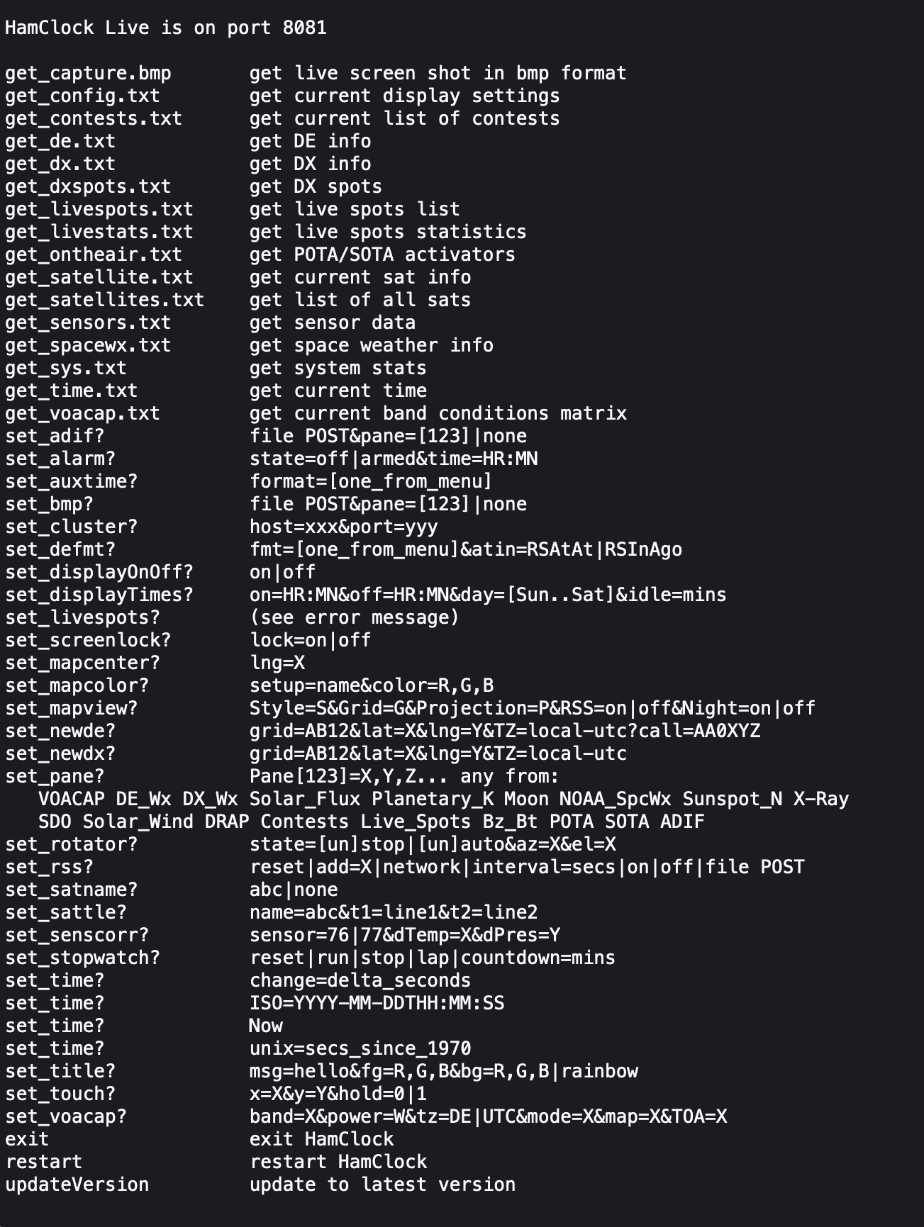
You can access the HAM Clock from another computer using a web browser pointed at your RaspberryPi on your local LAN using either the IP address or the hostname of the device.
http://<hostname>:8081/live.html

or

http://<ip-address>:8081/live.html
You can also control the HAM Clock remotely via web browser using a set of web commands that are detailed on port 8080 of the device.
http://<hostname or ip-address>:8080/
This is a great addition to any HAM shack especially if, like me you have an old HDTV on the wall of the shack that is crying out to display something useful.
More soon …
The RX-888 (Mk2) and external clocking
 |
| Figure 1: The RX-888 with external clock input (right) The enable/disable switch is barely visible behind the USB connector. Click on the image for a larger version. |
Adding an external clock connection
While the internal 27 MHz TCXO in the RX-888 (Mk2) is pretty good, there may be instances where one wishes better accuracy and stability. Fortunately, the RX-888 (Mk2) has provisions for doing so in the form of a jumper to disable the internal clock (when the jumper is removed) and a small connector (a tiny U.Fl) on board to accept that clock.
Unfortunately, it is up to the user to add the cable to feed an external clock - but short 4-6" (10-15cm) cables already fitted with a U.Fl male and SMA chassis-mount female connector are easily obtained from the likes of Amazon, EvilBay and others - just be sure that you do NOT get a "Reverse" (RP) SMA by mistake!
This leaves the jumper. While many people simply remove the jumper and mount the external clock connector between the HF and VHF inputs - or sometimes to the right of the USB connector knowing - from then on - their RX-888 will be unusable unless there is an external clock input - I prefer to make use of the ability of the internal clock to be switched - using (ahem) a switch allowing for testing/use of the RX-888 in a "stand alone" configuration - but this is up to you.
If one is careful, it's possible to mount the external clock SMA connector and switch on the same panel as the USB connector, orienting so that its handle is toward the "Clock In" connector to indicate that an external clock is to be used - but labels or markings are always nice, too!
If one takes the route of mounting the external clock input between the HF and UHF inputs, the switch could be placed to the right of the USB connector - or, if as in the case of one of my RX-888s where I put a heat sink on the FX3 chip and there wasn't room there - I found a very small toggle switch that just fit between the case screw and left side of the USB connector and tip of this switch may be spotted just behind the USB connector in Figure 1, above.
IMPORTANT: As the external clock input is simply wired in parallel with the internal 27 MHz clock. What this means is that with the internal clock enabled, it will be present on the external clock input. Similarly, if you supply a 27 MHz external clock without disabling the internal one, the two will "fight" each other and you'll get "garbage" results.
What type of signal to use as an external clock
While a capacitively-coupled 27 MHz sine wave is recommended for reasons that will be mentioned later, a lot of devices offer square wave outputs - and getting these to work reliably requires at least a little bit of attention.
Using the Leo Bodnar Precision GPS Clock to drive an RX-888:
Because the RX-888 natively requires a 27 MHz clock this means that if you already have a 10 MHz standard (GPS, Rubidium, etc.) kicking around, you will not be able to use it directly. While it's not too difficult to synthesize 27 MHz from 10 MHz (a number of Si5351-based devices can do this) it's most common for users of the RX-888 to use a device such as that sold by Leo Bodnar, which can be programmed for almost any frequency (from audio through UHF) with good precision and accuracy.
You can look at these products here: https://www.leobodnar.com (I have no stake in Bodnar, but I have used them and I and others have had good success.)
The most commonly-used device is the Bodnar "Mini" - which has one output - and this single output is often "daisy-chained" between RX-888s. There is also the functionally similar LB-1420 with a single output and the "Precision GPS Reference Clock" which has two signal outputs - but there is very limited ability to set the "second" output to a specific frequency and it's mostly useful for outputting the same frequency on the two ports - or outputting a 1PPS signals on the "unused" port.
Testing with a square wave - such as that produced by the Leo Bodnar GPS reference revealed that the drive level was far more finicky - and this has to do with the fact that a "square" wave with a reasonably fast rise time does NOT remain a square wave for very long as it quickly turns into something rather spiky and distorted as depicted in the image below:
 |
| Figure 2: A typical square wave output from a Bodnar GPS reference at the end of about 3 feet (1 meter) of unterminated cable. Ringing is evident! |
With
multiple "spikes" that can occur on such waveforms due to distortion,
it's possible - even likely - that certain combinations can result in
multiple triggering peaks of the waveform. In an extreme case, such
distortion can cause the Si5351 to be triggered at twice the
actual clock rate - but rather the result may be instability resulting
in the RX-888 clocking which can be manifest as anything from no signals
being "present" to those that are being off-frequency, varying, or just
"noisy" - and this errant behavior may vary with temperature and slight changes in operating voltage.
It's important to realize that like the RX-888, the Bodnar is ALSO DC-coupled which explains why the above waveform in Figure 2 largely rests above the center line (zero volts) with the exception of some "ringing" which extends negative and is likely being clamped somewhat by the '888's internal diodes.
With
a 3.3 volt waveform emanating from the Bodnar, we can reasonably expect
that - if the signal isn't too "ringy" that a signal exceeding about 1
volt positive just once per cycle is likely to trigger the 888's Si-5351 correctly.
IMPORTANT: If you try to directly drive an RX-888 with the output of a Bodnar, it will probably NOT work reliably! I have observed this with my own Bodnar/RX-888s and many others have reported the same issue.
Remembering that the external clock input of the '888 goes directly to very sensitive logic devices, a simple resistive attenuator pad will do double duty:
A 6 to 12 dB resistive pad - either 50 or 75 ohms - is a reasonable choice offering a bit of voltage reduction - but staying well above the 1 volt usability threshold - and such a pad, even if it is not connected to a 50 ohm load, will provide a bit of resistive termination, likely reducing the tenacity of reflections. While a resistive pad does not offer DC decoupling between the center pin of the '888's external clock input, it works with the Bodnar as that device sources a square wave referenced to zero volts so the pad simply acts as a voltage divider for that square wave.
Testing has shown that the '888 seems a bit more forgiving of signal drive levels if there is a DC blocking capacitor on its signal input - something that could be provided by placing a "DC block" device (available in SMA, BNC or F-type connectors) between the '888 and the external clock source.
Caveats and warnings - and why the '888 is so finicky about its external clock
The external clock input of the RX-888 - as described in better detail in the next section of this blog post - is connected DIRECTLY to inputs within the '888 and as such, it has a few undesirable properties:
Transformer-based signal isolation NOT recommended for the '888's clock input - sort of...
It is important for any receiver to minimize the amount of current circulating through the "ground" connections. Such currents in an analog receiver can induce hum in unbalanced audio lines and if the receiver is actually a transceiver, those same signal paths can induce RF into seemingly unrelated equipment in the ham shack.
Sometimes overlooked is the fact that these same currents can induce RF currents on the cables interconnecting equipment and it is likely that these will find their way into the receiver's front end and degrade performance by raising the noise floor. This is especially true when a computer-connect software-defined radio - like the RX-888 - is involved as we now have a connection (via the USB cable) to a device that is likely to be "noisy" at RF - namely the computer - but this also means that noise can come from other devices to which this computer is connected directly or indirectly, namely its power supply, other peripherals, its power supply - and noisy devices on the AC mains into which this power supply is plugged.
Current "balun"
For receiver RF connections one way to deal with this is to use a common-mode RF choke which is typically a dozen or so turns of coaxial cable wound on a T-140 or T-240 toroid - usually with 31 or 43 type material. This will break up common-mode currents on the cable - at least at HF - and can reduce such issues and this works for both the signal (antenna) and external clocking lines.
At DC and mains frequencies such chokes offer little/no efficacy and at low frequencies (below a MHz or so) these chokes lose their effective series resistance owing to limited inductance. What this means is that if you have strong circulating currents (e.g. current flowing between your antenna "ground" and house mains "ground") they will have little effect.
Voltage "balun"
A possible alternative is to use a transformer to couple between RF sources: A reliable, low-cost, commonly-available device for this is the Mini-Circuits Labs T1-1 which provides complete galvanic isolation between the source and load with a reasonable degree of longitudinal isolation.
 |
| Figure 3: A simple 10-ish dB resistive pad with DC blocking to keep the external clock input of the RX-888 "happy" and to prevent clipping of negative-going voltage by built-in protection diodes. The "small" capacitor value also minimized the amount of stored charge dumped into the '888 due handling/shorting of the input cable. |
 | |
| Figure 4: This circuit provides both common-mode isolation and a degree of band-pass filtering of the 27 MHz clock signal: Filtering to a sine-like waveform reduces glitching due to cabling issues (reflections, misterminations) as well as offers a degree of protection to the RX-888's input as the filter will limit the amount of energy that could be imparted. It also provides a (small) degree of termination (<150 ohms). The "optional" 1000pF capacitor shunts low level leakage of the 27 MHz signal due to transformer imbalance - but it is suggested that one use a common-mode choke to restore isolation at HF frequencies. |
This device is slightly more complicated, but it offers several advantages:
 |
| Figure 5: The (nearly) sine wave output from the circuit depicted in Figure 4. Click on the image for a larger version. |
The disadvantage of this circuit is that it requires the winding of a toroidal transformer and tuning it to 27 MHz - something easily done with a NanoVNA or an oscilloscope and an oscillator.
Figure 5 shows the resulting waveform that has passed through the circuit depicted in Figure 4: It is nearly a sine wave and as such, it is much more resistant to causing false triggering on "ringing" edges as compared to a square wave.
 |
| Figure 6: The prototype transformer/filter circuit depicted in Figure 4 connected at the Bodnar, connected to the '888 with a short BNC<>SMA jumper. Click on the image for a larger version. |
Figure 6 shows the circuit of Figure 4 in action, connected directly to the Bodnar's output and - via a very short BNC to SMA cable - to the RX-888 sitting atop it.
This prototype unit was built in a piece of copper-clad PC board material. On the top side, the components were wired with flying leads to the connectors and "dead bug" on the copper itself: Between the "Bodnar" and the "RX-888" side the copper was cut to provide the two separate signal "grounds" with only the transformer coupling between the two.
At some point, it may be worth designing a small PC board for this, but for the meantime a small number of these prototypes have been built and put into service very successfully. As suggested earlier, the a step attenuator was inserted between the Bodnar and this circuit and the signal reduced until the '888 no longer reliable locked to the external clock and it was found that there was plenty of margin to assure stable operation under varying conditions.
Lots of other possibilities
Now that you know what the RX-888 "wants", you have a better idea of what you are likely to be able to "safely" use to drive the external clock input of the RX-888.
* * * * *
This page stolen from ka7oei.blogspot.com
[End]

 |
| Front panel design by W4OA. 3D print design files on github. |


For some years I’d been aware of HamClock and around April last year I decided to investigate further and built one using an old Raspberry Pi 3B that I had spare.If you’ve never heard of HamClock, it’s described on the authors page thus: “HamClock is a kiosk-style application that provides real time space weather, radio […]
The post HamClock first appeared on QSO365.
There is a total of 10 different bars and here are the two which are used in the upcoming version of the Multi face GPS Clock.

This excludes some fancier bars that require more or less continuous updates of character sets during progression of the bar.
The code and images of the other eight bars can be found on Github.

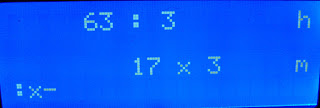
A brief press on the rotary encoder will enter the setup menu with these options:
< 0 Clock subset >, < 1 Backlight >, < 2 Date format >, < 3 Time zone >, < 4 Local language >, <5 Secondary menu>.
Submenus will lead the user to :
Chosen values will be stored in EEPROM so next time the clock is started it will start with the values used in the previous session.
A long press will reset the clock.
The code can be found on Github.

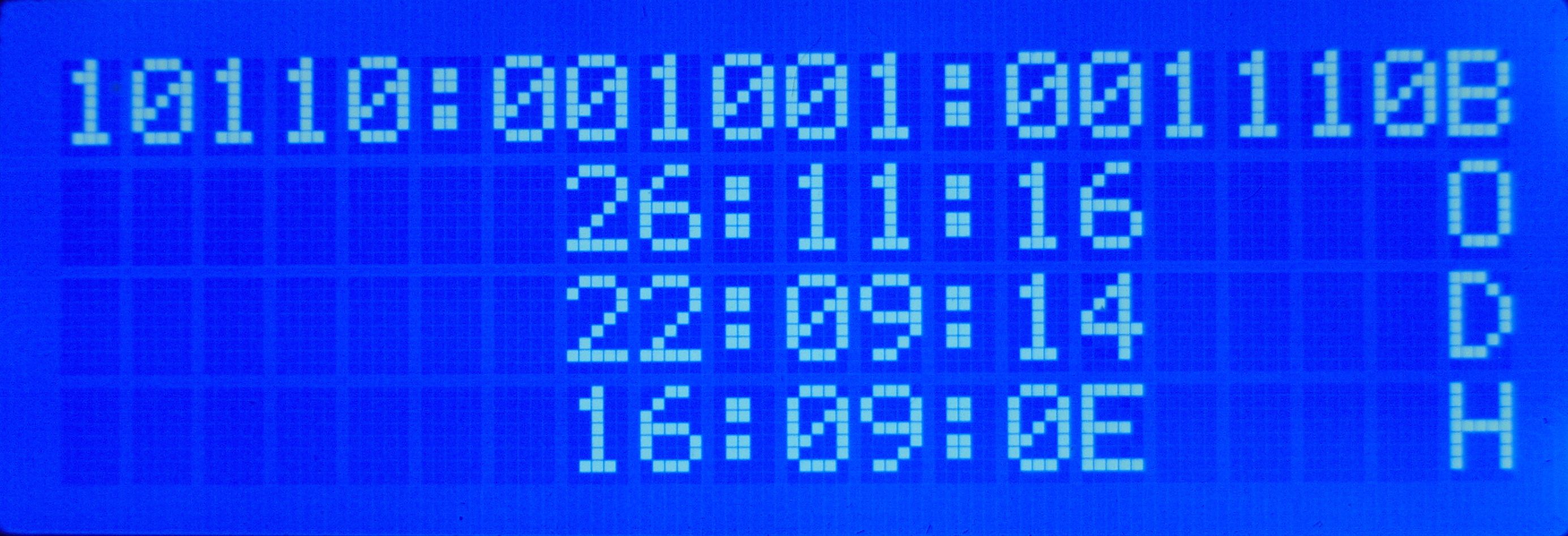
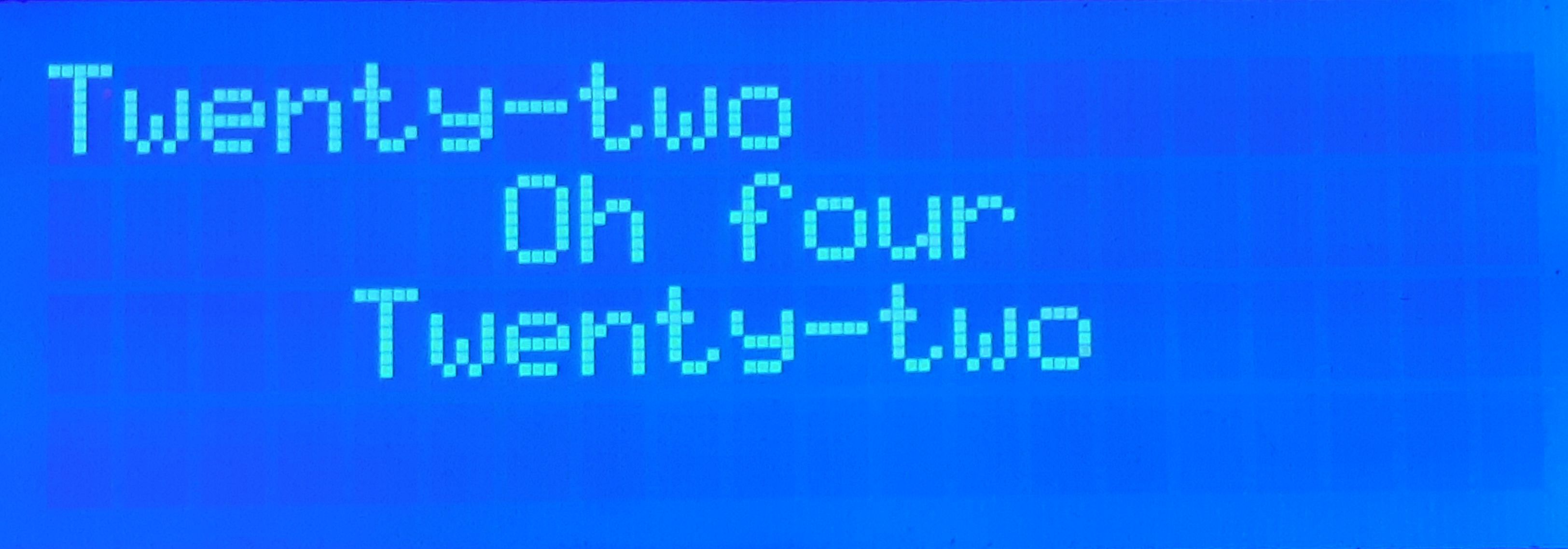
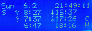
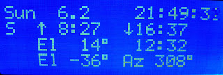
This is screen number 39 for this clock, all of them selectable by rotating a rotary encoder. The project, with Arduino Mega hardware and software is documented on Github, where the current release is v.1.6.0 (2023-04-14).
The display also shows the full name for the element corresponding to the second, as shown above for element 3 which is Lithium. It is located in group (column) 1 and period (row) 2.


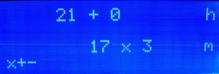
The multi-face Arduino GPS clock is inspired by the Clock Kit from QRPLabs. It is an open source project on GitHub, and it now has support for many more languages in the newly released versjon 1.4.0. As a language nerd myself, I love fiddling with multiple languages and character sets.
The local language option is for display of day name in case local time is shown. The default is English for local time. No matter the choice for local time, English is always used for UTC day name. Here are examples:
French:


Main links for documentation


The Norwegian Ham meeting 2022 will take place 11-13 March near Oslo Airport Gardermoen. Norwegian and some Swedish radio amateurs will meet and the program is here (Norwegian). It will be nice finally to meet again!
I will give a presentation on Saturday morning: "An easy-to-build GPS clock for the shack".


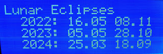

The GPSClock from last month has now been updated and software version 1.10 1.1.0 is available on Github. The main upgrade is the possibility to use a rotary encoder for selecting display screen or clock face.
In addition a new screen showing Easter for the next three years, according to both the Gregorian (Western) and Julian (Eastern) calendars, has been added as number 22. The dates are shown in the Gregorian calendar: