I have been busy with some other things that have kept me away from electronics projects for quite a while. Now I can get back to them, but realize I need some boxes to put them in. I have 3D printed some simple ones a while ago, I will redo the design to make them fit the way I have been building my projects now. Most of my designs use modules that I etch or route. For these I buy copper clad boards that are usually 100 mm wide. This is one of the standard widths availibale cheaply through eBay or other suppliers. One standard size I use is 100 x 70 mm. Going with that as a default I designed a clam shell case, that has two identical parts, that you join together with a few screws. I want to be able to simply add modules without having to drill holes in the case.
To do this I designed the case half with slots to slide the modules in vertically. After printing a set of these I decided to also design another without the slots to use as a top, which makes it easier when trying to aligning multiple modules.
I decided on 7 internal slots for modules, along with slots on the ends for front and rear panels. I also made versions in three heights, mixing different height versions I could get an inside height from 40 to 80 mm. in 10 mm steps.
I also made a set that fits one of the standard 50 x 70 mm perf boards I use sometime. This one only has 4 internal slots long with the ones on the ends.
I made the mounting holes to fit 3 mm screws. They are tight but I was able to self tap without too much problem. Depending on printer settings and filament I might have to run a drill bit or a tap through the holes to clean them up.
For those interested I have added the .stl files to the dropbox I have for the storage boxes from a previous post.
Unfortunatly I was not able to make it to FDIM this year, but was able to watch the streamed presentations. All of themwere good, but the one tht interested me the most was Farhans' DAYLIGHT RADIO. The design is interesting because the input and ouput impedances of the different stages were not all designed to be at 50 ohms. This can make the design a little easier in some cases.
Farhans' design is for an all analog system including the VFO. Not sure if I will go that way or use a micro-controller and a SI 5351 instead. There are some ideas I want to try that would require the micro-controller. But if everything is in modules, they can be swapped out with the analog stages as desired. If I went with the Analog VFO I still have enough parts to use one of the small frequency counter boards I built up years ago.
Lets start with the AF Filter and amplifier. Farhan has a nice desription in his presentation so I will just ashow his schematic. Everything is the same except I am using seperate opamps for the AF amplifier, and the product detector. Because of this I shorted the unused opamp + input to the common reference used by the AF amplifier, and the - input to the output . This is left to float, and as just a precaution to prevent any possible instability of the unused opamp from affecting the AF amp.
I laid out the board using through hole components, but I might make another using MUPPET style, or shrink it down even more and use SMD components.
I will etch the board using Toner Transfer, but since I also have a CNC I can use it to pre-drill all the holes. Then it is very quick to align the toner image to the board using the holes as s guide. This makes the whole process very quick and easy.
Since the board is fairly siimple I decided not to bother with doing a silk-screen . If wanted I could just print it on a laser printer, and iron this on the same way as you apply the toner image for etching.
This board turned out pretty nice, so now I can finish the layout of the product detector and balanced modulator board, and get them built.
With as long as it takes to get some of the components these days, it is nice to have several home brew projects going. at the same timr. And speaking of home brew, I have a two gallon batch of beer ready to bottle.. Thats always handy to have on hand when it takes toooooo long for the electronic components to arrive.
Getting back to workingon the VWS DC Receiver, I decided to combine the AF mplifier and the low noise amplifier on the same board to cut down on size. Because I have been thinking about having separate Low Pass filters for SSB and CW, I will put them on another circuit board instead of with the LNA.
To better match the low impedance of the of the Low Pass filter, the LNA uses a common base amplifier feeding a common emitter stage. To provide power supply decoupling, Q2 and the associated components are commonly called a cpacitance multiplier. This provides a capacitance value to the input stage of approximatly the value of C3 times the gain of Q2.
This configuration along with the LM-386 stage has over 90 dB. total gain, therefore a separate gain adjustment is added to prevent possible overload distorton.
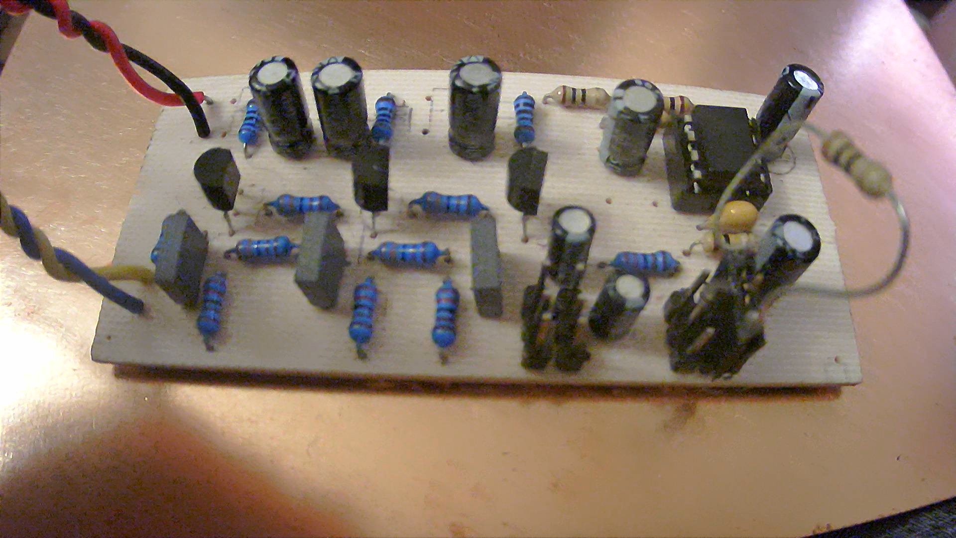
I decided to make the board MUPPET style, instead of using through hole. To reduce the board size I installed the resistors vertically. I
etched a board using toner transfer, and dipped it in some 'liquid tin' to provide a better soldering surface than just bare coppper. One of these days I will try one using the CNC router to see if there is much of a difference in the quality I can get.
Waiting on an assortment of inductors, that seem to be taking forever to get here so I can finish the LowPass filter board.
I have been working on several projects, most of them not related to electronics. The main electronic related one has made me look back on some code I wrote 6 years ago when I first started learing C++ and the Arduino IDE. Still wonder what I was thinking of, and how did I ever get anything to work. Looking at some of the code made me think it was written in a write-only languge. Almost as bad as looking at some of the things written in FORTH.
I had been following the Vienna Wireless Society makers group and their Simple SSB transceiver. They finished that with around 10 units up and running. Many built by members that had no building expereience. I had started to build a version of this, but they had mostly finished with the project when I started joining their Zoom meetings. I had some ideas of how I would like to change this, and then other things came up that postponed my doing this. They just started a new project, to try to get more of their club members into home brewing (electronic kind not liquid kind). This one is a Direct Conversion Receiver which should be easier for the first time builders.
I am going to try to follow along with their progress, and build each module as they are presented. Probably make a few changes as they progress to reflect some things I already have on hand. They have a Zoom meeting about every other week, to present info on the next stage in the project, keep up with build progress, and provide assistance as needed.
This is a fairly conventional DC Receiver. The interesting thing is that they plan on using a home made Diode Ring Double Mixer, instead of a ADE-1, SBL-1. or an active mixer like the NE602.
Here is the block diagram of the receiver, with each block being built as a separate module. Many of these blocks are similar or the same as used in their SSSB project. so there should be plenty support for the first timers available if needed. They plan on using an Arduino and SI5351 as the VFO, but one of the members has already built an analog PTO that could be used instead.
Their last Zoom meeting went over the block diagram. And, a gain distrabution diagram to define the gain or loss in each stage to get up to the required overall system gain.
Then went into the first module to be built. This is a basic LM386 AF amplifier circuit taken directly from the LM386 datasheet. Nearly the same as used in most all simple receivers. The only thing that is slightly different, is a variable resistor in series with the gain determining feed back capacitor. Since almost all of the overall gain is in the AF amplifier stage, this resistor allows you to set the final stage gain to prevent clipping on strong signals with the volume control all the way up.
Most of the modules will be built manhatten style using MePads, but any other type of construction would be fine. Since this is all at audio frequencies, a ground plane is not necessary and it could easily be built using perf bard. This would be similar to the final stage of the version in my previous post.
I used some simple PCB layout software to position all the parts for easy building either with the pads, or to route or etch a board instead. This allows me to make a smaller bard than just eye-balling the parts placement on a bare bard. One thing that I did different from the diagram is swap connections to the plus and minus pins (2,3) on the LM386 That just made layout a little simpler. Since the LM386 has a differential input it will not change operation.
The board turned out very nice. Not as small as could be done by using proto board, or doing a through hole PCB. But, was faster than either of those two metnods, and should be fairly easy for the first time builder. When I get a little time, I will do some testing on the board and see what the actual stage gain is, and how much it can be varried with the resistor.
Should be another group meeting later this week to see how everyone is coming along. Will keep you updated on the next stage in the project.
I have done several versions of VFO/BFO circuits using differentmicrocntrolers. Any of these would work for the Simple SSB transceiver. Looking at these, you can see that they are also very similar to some of the test equipment I have previously built. I know that some people who are interested in building this transceiver, have very little in the way of RF test equipment. So why not build something that can be used to test the modules as they are being built, and then as the Controller,VFO/BFO to finish off the project.
Doing something similar to the test gadget from a couple years ago, I went with a basic Arduino Nano, the SI5351 module, and a TFT Display. To this I added header pins to bring out pins for a Rotary encoder and other controlls. To an expansion header I brought out DC power, analog, I2C , and the SI5351 clock lines. Since some of the TFT Display modules require 3.3 volt logic levels instead of the 5 volt out of the Nano, I added 1K resistors in the control lines to provide current limit for the display if using a 3.3 v module.
This also helped make the layout a little easier. After a number of tries I was able to get the layout to fit on one of the 50 x 70 mm perfboard in the kit I purchased. When building this module I found that it worked quite well to bring the wired up from the bottom of the board and run them across the top and back down to connect at the other end. Doing this kept the board fairly neat. The only insulated jumpers I had to install were to bring the 5V line across the expansion header. This layout would also work well for etching or routing a single sided circuit board.
After building the board, the only thing I had to do to one of the early Arduino sketches I had for a simple VFO/BFO was to change a couple pin definitions for the SPI lines going to the TFT display. This made a fairly compact board that can be easily mounted, with a connecting cable going to the rotary encoder and several switches on the control panel.
Since I also want to be able to use this as a test_set during construction of the RF stages. I built up a small board with a rotary encoder and 3 push button switches that plugs on to the control header pins on the Arduino controller board.
Looking back at the Sweepering Jr., and different versions of the SNA Jr. projects, I decided to go with much of the original SNA Jr. design. I built a simple add on module that can be used asa Sig.Gen., SNA, RF voltmeter.
I bring out two of the SI5351 clock outputs throughs DC locking capacitors, one of them has a 50 ohm load placed across the output. This can be used as a two channel signal generator. There is limited level control, but you can build very simple attenuators to take care of that issue. Instead of using an AD8307 Log amplifier for RF measurements, it used a 1N60P shunt diode detector feeding a MCP6002 operatinal amplifier. This two channel op-amp is very nice to work with in microcontroller circuits. It only requires a single ended power supply, and works well at 5 volts. It has rail to rail output, so you can use the whole 5 volt input range of the Arduino Nano. They are readily available in 8 pin DIP and SMD versions, and are less than $1 through most suppliers. This circuit does not have the sensitivity or dynamic range of an AD8307. But, for use as a RF voltmeter or in a SNA over the range of voltages expected in testing the transceiver it will be very adequate. One of the detectors has a 50 ohm load on the input for power measurements or use as an input for the SNA function. The other is configured as a remote RF probe with a x1/x10 voltage divider, for basic RF level checking.
Just like other parts of the project,
the test set options will be built as simple modules.The test set modules will plug onto the 18 pin expansion header on the VFO/BFO board. It is built on one of the 50x70 mm. boards in the kit I purchased. You can use edge mount SMA connectors for all, but I substituted 3 pin right angle heder pins for the RF probe connection, so I could use it for other possible functions. A 3 pin keeps the layout the same for either, and makes a more solid feeling connection.
Adding an adapter board for the TFT display and making a simple 3D printed sleve to hold everything, the modules plugged together make afairly compact test set.
Now to finish the software. It will have parts from the SNA Jr., 2 channel signal generator, and Sweeperino Jr. projects, plus a couple more if I can fit them all in the Nano.
I hope to have several other modules that such as an antenna nalyzer. SWR power meter. measurement receiver, and possibly a very simple Spectrum Analyzer for up to about 60 MHz. These will be added as the transceiver project progresses.
After finishing the microphone amplifier and the AF amplifier modules, it is time to test them. For the experienced builder with scope and signal generator available it is no problem. If you are new to building, and don't have these available, there is a very inexpensive option that may even work better.
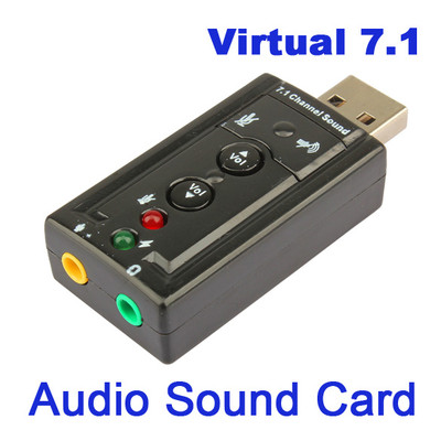
I spent more than 25 years working as a field service technician. During this I spent more time than I want to think of dragging scopes, and other pieces of test euipment around. During the last years before I retired, I found several useful pieces of software that allowed you to use PC sound cards as scopes and or signal generators. Although they were not suitable for calibrating the equipment I worked on. They were more than adequate for trouble shooting, and verifying basic system operation
Although these worked better with actual sound cards, they also work quite well with the very inexpensive USB sound cards that are available simular to this one.
Other USB sound cards will give more options such as dual channel input, but are more expensive.
Only prblem I have found with the USB card is that sometimes there are higher frequency signals found because of traffic on the USB bus. This has normally been higher than the 5 KHz. I think of as the upper limit for frequency response in comunication equipment.
They only requite a simple interface to provide usable results. I have tried several, from basically just DC blocking capacitors,to ones with internal amplification.
The one I use most of the time uses a simple X1, X10 voltage divider along with DC blcking capacitors on the output to the MIC input on the sound card. If you use an internal sound card with a Line Input, you can build a two channel version of the interface.
If you use Line Input you can elminate the DC blocking capacitor going into the sound card. It is there to remove the DC voltage out of the MIC input used to power Electoret microphones and provides protection for the sound card. I like having some protection for the sound card from DC voltages in the circuit being tested. Espically if you use this to test Tube circuits, with their higher voltages. To add this place a pair of back to back diodes 1N4148 orsimilar across the input to the sound card to ground.
For the Signal generator output, I capacitivly couple the sound card stereo channels to a 1K pot. This couples the L and R channels , and lets you ballance the output levels so you can use this to generate a two tone audio signal for testing transmitter out settings. The combined output then goes to a Pot. for level adjustment and a DC blocking capacitor to the output connector.
This is also built with perf board, and use right angle header pins as output connectors. The header pins let me use JST jumpers to connect to modules being tested or to build simple fixtures for making testing easier. Instead of a switch I use a 3 pin header and jumper to selecdt voltage level. You could also replace the voltage divider with a 1 Meg. Pot. to make construction even easier. I used some 3.5 mm. jacks for the signals going to the sound card. You could elminate them and use a 3.5 mm stereo cable cut in half and wired directly to the circuit.
Visual analyzer has additional functions among them a Voltmeter, Frequency Meter, with additional hardware a ZLRC meter.
Both free for non commercial use, a commercial license or donation available.
I am only going to use Soundcard Oscilloscope for this post. After doing the install you get the main screen.
Functions are selected from a set of tabs above the scope display. First thing you need to do is select your input and output device, and set the scope paramateurs. Amplitude calibration can be done later. For ease of learning the interface select scope loopback for input and output device
First function to check out is the Oscilloscope function selected by clicking on the first tab. To the right you have controls for setting the voltage range per channel and the timebase for the sweep. There are also options for setting trigger type , slope, and threshold.
Just below th display area there is a button to set the type of measurement you can make. You can set cursors for both amplitude and time. For both there is a display value for the reference cursor and the difference between it and the second.
The next thing to look at is the
signal generator tab. This allows you to select the type of signal generated, frequency and amplitude for each channel. It also allows you to set up frequency sweeps that are very handy for checking frequency response of amplifiers. This can be brought out as a separate window to make it easier to use.
The last function I commonly use is the frequency display. This uses a FFT to compute a spectrum display of the input signal in the frequency domain, instead of the time domain. This is very useful for measuring the frequency response of a audio amplifier or filter, when used with the signal generator. You can place a cursor on a signal to get the frequency of the signal. Along with the cursor you can use the zoom function and position to look at a signal in more detail. Unfortunatly there is no vertical cursor, so you have to turn on the grid and reference signal levels to a scale on the side. Some of the other useful options in this function is the ability to look at the levels in dB, and usea peak hold when sweeping to plot the frequency response of a amp or filter.
One common way to check frequency response, is to set the signal generator start frequency, turn on sweep and set the end frequency and sweep time. I usually set the end frequency to about twice the highest frequency response I am trying to measure. Then on the frequency display set peak hold and set to dB and auto scale. Let it run a few passes and you have a good indication of the frequency response of the amp or filter. Do this with two different signal levels and you can find the gain or loss of the device being tested.
Another method to measure frequency response is to select White Noise as the signal being generated. On the frequency display panel everything is set the same. After a few passes the frequency response shold be clearly seen. Make sure you use White Noise and not Pink Noise. White Noise has a constant amplitude over the whole audio frequency range, where with Pink Noise the amplitude fall off as frequency increases. For checking frequency response it can show a incorrect result at higher frequencies.
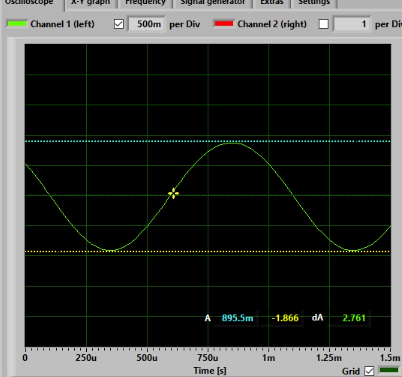
Now lets switch to the sound card input and output, and connect to the microphone amplifier. After setting the signal to a 1KHz Sine wave and a level just before the output started to distort.
I switched to the frequency mode and set the signal generator to sweep from 20HZ. to 20KHz. With the display in dB and max hold, you can see the frequency response is flat from 100 Hz to over 10KHz.
The log display makes it look noisier at the higher frequencies. But, if you look at the response you see that the noise level is fairly constant across the whole range.
There is one alignment of the test fixture that should be made, that is to adjust the balance between the two channels. This signal will be used later to do a two tone test for setting the microphone level. A good Youtube video by W2AEW Two-tone test of SSB transmitter output explains the test quite well. The two frequencies should be non-harmonically related and adjust the balance for equal levels. I used 750 and 1250 Hz. and set the cursor at 1000Hz. Then use the zoom control to spread the traces apart. Then just adjust the balance pot for equal amplitude. Make sure you have peak hold turned off while doing this.
Testing the audio amplifier module is the same as the mic. amplifier. Only thing different is that you need a load between 4 to 32 ohms on the output. The first stage of the audio amp. is nearly identical to the mic. amp., it is followed with a LM386 AF amp IC. The volume control should be a audio taper pot, but I only had linear taper in my parts box. You can approximate an audio taper by adding a resistor between the wiper and ground terminals on the pot. You need to use a larger value pot. to compensate for the final parallel resistance. Normally the added resistor value is around 20% of the pot. value. I ended up using a 20K pot and a 3K9 resistor.
Setting things up the same as for the mic. amp., 1 KHz. sine wave set the input level and volume control to just below the point of distortion on the output signal. This is kind of tricky because of the gain of the LM386 is set quite high and you can get the output to distort very easily. I turned on the sweep from 200 Hz. to 20 KHz. and let it run for a while with peak hold turned on. I got a linear response from 200 to just over 8 KHz. where it started to drop off a little. Overall the AF stage has quite a bit of gain, that can start to distort fairly quickly, but has a flat response over the frequency range of interest for communications equipment. Gain on the LM386 can be reduced by decreasing the value of th capacitor between pins 1 and 8 of the IC, if desired. Thats it for testing audio amplifier stages. AF filter response can be tested iin the same way.
Next I will work on the VFO-BFO oscillator, based on a SI5351 module and Arduino. I have done several versions of these before, but will layout a simple version that can easily be built on the same style perf boards. I plan on bringing pins out that will allow the module to be used for testing RF stages in the transceiver. Hopefully I can get this to work similar to the original SNA Jr. or Sweeperino from my earlier posts. This should be very helpful for those who do not have anything in the way of RF test equipment.
I had decided to build most of the transceiver using perf board. I prefer the double sided plated through hole variety to the bare variety. For me it just makes it easier to solder the part in place, and then route the leads as needed. Also if you have to replace a part, you can usually just clip it off on the top and solder in a replacement without changing the connections on the bottom.
This type is available in various sizes. You can find small kits with several small sizes for around $10. You can also get larger size boards and cut to the size desired.
After I received the kit, I changed the layout to fit one of the sizes in the kit. The extra time spent making an exact layout template really saves time, and frustration in the long run. I also did the layout in ME Pad and Muppet format, and all are available at
When I first started building some of my projects, I used many components I had salvaged from junked equipment, or surplus supliers. Anyone remember 'PolyPacks' ? Because of this I got into the habit of always measuring the value of the components as I used them. Time spent doing this also paid for itself many times over. Now I use better quality parts, but still test them before use. Getting harder to read the values on these small parts for some reason.
For this I use one of the inexpensive component testers available through the usual suppliers. The one usually use is similar to this one, and has pads for use in testing SMC components. They are available with or without cases for $10 - $20. Most of them measure R,L,C, along with diodes, transistors and FETs. For the seimconductors, they give pinout along with values such as gain and internal capacitance depending on type being tested. The first one I bought did not have a case so I found the design for a 3D printed one.
Following the template, it only took a little while to do the actual construction. For audio and digital boards I use either straight or right angle header pins for connectors. This allows me to use JST style jumpers for wiring for DC and control signals. You can also add connectors to shielded cable if needed. Or, you can easily solder wires directly to the pins if desired. For much of my test gear, I have adapters made up so I can use JST jumpers for ease of testing modules.
Now that this module is finished, I did a layout template for the AF amplifier. Since the premap half of the AF amp is nearly identical to the Mic amp, I could just move components over a little to make room for the LM-386 and associated components.
It turned out like this. This was fairly crowded on this size board, so I did another template using a slightly larger board in the kit. This one allows plenty of room for components. Either version will work. Just up to the builder to choose the one they prefer.
I also did a ME Pad template for those that like that construction method. but only for the smaller size board. They are available at
Normally I would start with the audio amplifier board, but in this case I will start with the microphone amplifier for two reasns. First it is the simpelest to build, and second almost all the other circuits in the transceiver are just a variation of the same common emitter amplifier. Values have been changed to provide different gains, or frequency response. For the RF stages. compnents have been added to provide impedance transformation to make it easier to connect to the next stage. If you look, the bi-directional amplifiers in the IF stage are basically two common emitter amplifiers on top of each other. Switching power to the desired amplifier changes the direction of signal flow.
The schematic and values are directly from the LT Spice simulation by Pete, with the exception of an added 100K resistor that can be jumpered in if you need to power an electoret micrphone. For a lot more informationon how the values are determained check this YouTube by Charlie ZL2CTM on Common Emitter Amplifier design If you have not already checked Charlie's YouTube channel you are missing out on a huge amunt of information. He has built a variety of both hardware and software defined radios. He goes into the the math required for the design in a lot more detail than I even want to think about.
I have tried many different construction methods over the year, and have found that time spent doing the inital layout, can save much more time and effort in the actual build. I have tried 'Ugly' or 'Dead Bug' , I find that it quickly turns into something that is impossible to modify if necessry. At least for me, I have seen some fantastic builds that others have done. I perfer using a Perf-board for one off AF or RF circuits, and for almmost all Digital circuits.
I started just doing the layout with pencil and paper, but still ended up running out of room or needing to use a lot of jumpers. A few years ago I started using PCB design software, and now use it no mattr what method of construction I will be doing. There are two main types of PCB design software. One ties the PCB layout directly to a schematic. This offers more assurance that the layout will be correct according to the schematic. The disavantage is that if you want to make a change to a component or value on the layout you will have to go and make the change in the schematic first. The other type is more of just a graphic design program that allows you to add or change components in the layout as you want. This means that the entire correctness of the layout is up to you.
But depending on the software, this method has some major advantages. The software I usually use allows me to take part of an existing layout and save the entire section as a component in the library. Most of the other programs I have tried allow you to make new components, but will not allow you to save a part of a layout as a component.
One of the design programs sometimes I use is ExpressPCB+. It is free but tied to a single board house. You do not have to option to export as a Gerber file that can be sent to any PCB house. For those who make their own PCBs using the toner transfer or other metods can use the printed output of the program to make the transfer image. My favorite proram is Sprint Layout, not free but only around $50. It has all the options of ExpressPCB+, and the ability to generate Gerber files along with many other features.
First thing I do is design the board as if I was going to make a simple through hole PCB. I can easily move components around to fit the size board I want, simplify layout, and elminate as many corssing lines as possible. I could generate the image to use for toner transfer and etch a board, use a cnc router to mill the board If I set the grid size to be .1" (2.54mm) I can use it as the layout template for a perf-board build. They will look something like this.
For RF and digital circuits it is often desired to have a large ground plane on the board. In this case the software allows you to fill the board with a copper pour, and isolate the traces and component pads that are not connected to ground. This can be either etched or isolation routed. In this example I show the ground trace just as reference, It is really through the copper pour that the grounds are connected. On more complicated boards this can be a problem if component and trace layout isolate ground from one area of the board to another. In this case jumpers may be necessary, or a double sided board with 'vias' to connect the ground sections together.
These two examples use through hole components, and for the hobbiest that means a lot of drilling. To make this simpler for the another method called 'MUPPET' has been developed. this moves the copper traces from the bottom of the board to the top. Instead of pads around the through holes, a large solder pad is placed at the end of each component lead. It is fairly easy to bend the component lead sso it can be soldered to the board. Ground connections go directly to the copper .
For those who do not want to take itme to etch boards, another method called the 'Manhatten Method' is very common. It uses small pads made from copper clad circuit board gluded to a piece of bare copper PCB material. These pads may be home made, or a commercial product called 'ME Pads' are available.The things you have to watch for is that any adjoing pads are properly jumpered, and that connected pads should be jumpered with insulated wire to prevent shorting to the ground plane. This method has the advantage of being very quick and the template looks something like this.
Another common method used is to create 'islands' on the bare copper PCB material witha CNC router, or manually by using a tool such as a 'Plexiglass cutter' to scrape lines through the copper PCB material. The most important thing if done manyally is to make sure all the copper material is cleared away, and there is no connection between the islands. This could also be etched if desired. Again the traces are shown only for reference, the components are soldered directly to the PCB 'islands'.
From these simple examples, you can see that the same layout can be used as a template no matter which method you want to use. There are several other methods using things like strip boards that are used by very successful builders . Look around on YouTube, and you can get more information on many of these methods. Some of my earlier posts cover toner transfer PCBs and might be helpful.
So no matter what method you want to use for the project, my reccomendation is to play with the layout using whatever PCB design program you want and simplify the layout as much as possible before you heat up a soldering iron.
Now I have a useable template for a perf-board version, and a package of parts just arrived yesterday so I can get started on the mic amp. Next post will look at how it is built and some simple ways to test it and the AF amplifier module that comes next.
Those that have been following my blog for a while, know that I am a fan of Pete Juliano,N6QW, and his MANY transceiver projects. Recently on the SolderSmoke blog, there was a post about one of Pete's project being built by group of amateurs belonging to the Vienna Wireless Society in Virginia.
A member of my local QRP club posted this to our groups.io page, and there were several people that were interested in building one. I contacted Pete, and he put me in touch with Dean KK4DAS. Dean is the one leading the group at VWS through the construction of around twenty SSB transceivers. As of now almost half of the group have their project up to a working receiver.
The other evening I was able to join their group in a Zoom meeting. They went over their progress. and shared information on the next stage in the build. I have also spent a lot of time going through the documentation they have been creating on theVWS Makers Group SimpleSSB Project page. Some of the information there covers the module layout they used, some simple test equipment needed, and software developed. Dean has added to the oritional software, to provide support for different display types, and added features like CAT control.
Several of the members of my local club interested in this project have only experience building some of the kits available through the common QRP sites. They feel that they would need quite a bit of detailed information to build something from just parts. I decided I will start working on a series of blog posts that will document the build in a detailed way that can fairly easily be copied by someone with very little or no experience. I know that most of these members have very little in the way of the test equipment that would be helpful in a project of this type. In these posts I also plan on describing some very inexpensive or easy to build test equipment. And, I plan on adding some test functions into the transceiver itself. A lot of the test equipment information will be a reference to or revisions to what I have covered previously in this blog.
Most of the design is based on the work of Pete N6QW and can be reffenced at the links in his blog. N6QW.BLOGSPOT.COM
Some of the minor mods I have made are based on some of the things I learned watchingCharlie Morris ZL2CTMYouTube Videos. For those who have not seen any of Charlie's videos, he goes through in great detail the math involved in the design of his circuit design. Also incorporating the info from Dean and the VWS group, and some of my own ideas and preferences.
There are several options commonly used for buildiing a project of this type. Manhatten or MePad, Perf-board, CNC Routing, and the one I use quite a lot Toner transfer etching. For this I will use perf-board for most of the modules. My preference is using double sided boards with plated through holes. There are several inexpensive kits available with an assortment of sizes for a very reasonable price. These small boards are ideal for building individual modules. The probem many new builders find is getting the layout so it is easy to build. I perfer to use a PCB design program with the layout grid set to the .1" of the perf-board. This makes it easy to move things around to get a nice neat layout that is easy to duplicate. Then it is easy to transfer this to the perf-board for the actual construction. With this layout I can also generate files for Toner Transfer etching, or CNC routing. Even Gerber files if one desires to have boards made by one of the inexpensive board hoses in China.
These are my plans for the next few posts. If anyone else would be interested in this project contact me directly at duwayne@kv4qb.us. With most people now familiar with Zoom and Jitsi meetings, it would be possible to schedule meetings for everyone to get together and work as a group.
Not I need to go check my parts bins and see what extra stuff if any I need to order.
While getting some equipment off a shelf I knocked some thing down and they landed on a nanoVNA, cracking the screen.
I think it is time to make some protetive cases for the equipment when not in use. Looking around on Thingiverse I found a small case that is similar to to a Pelian Case. I printed one and fund it to be exatly what I wanted. It is very strong with a nice latch system that closes very tightly. It has a seal that can be made watertight if I run a small bead of silicon tub sealant in the grove in the bottom part of the box. Or there is a seal that can be printed using flexible filament.
Using this basic design and dimensins for the hinge and latch mounts, I designed several more boxes of the sizes I need for some of my other instruments. With this design I can use the same lacth and hinge parts as the original design.
I printed these up using some HIPS, PLA or PETG for the case top and bottom. These all worked quite well, with the PETG probably providing a little tighter seal. I found that PETG worked best for the hinge and latch parts. Since it is slightly flexible it holds the two parts of the case tighger than ones I printed with of PLA.
I lined the inside of a case with some mediam density foam to hold the instruments in place and provide quite a bit of protection.
I am going to try to design some printed inserts for some of my other instruments instead of making them out of foam.
After I clean up some of the cad fies I will post all of then for anyone interested.
Original box design on thingiverse
https://www.thingiverse.com/thing:4094861
Use the latch and hinge components for all other designs
Update
Designed and printed a new box bottom for a NanoVNA. This has built in compartments to hold the VNA , cables, and cal standards. I use connector savers on my VNA, so had to make the compartment a little longer. This gives me room to also store my printed torque wrench. Will have to print one for my other nanoVNA. With a piece of foam in the topccover, everything stays in place.
Still need to play with some of the printer settings. So far it looks like I need to use about 15% simple grid infill to keep the weight down. And 3 perimiter layers and 5 top and bottom layers.
Still checking and cleaning up the CAD files. Since I am using a fairly old commercial CAD program that does not use a standard file format for the raw file I will be exporting them to .stl format. As I check the CAD files I will store the .stl to this dropbox folder.
Well it has been a while since I did an update post for the TinySA or anything else. It has been a combination of some computer problems that I had to correct along with the associated data recovery. I also made a mistake and bought a FireStick for my TV. With all the streaing channels available it is WAY TOO EASY to spend a lot of time watching some of the older movies and TV shows. I have also been doing a little bit of another type of Home Brewing. Just finished up the 2nd. generation batch of UJSSM, and starting on the 3rd. generation.
So, lets get back to the TinySA. There has been quite a bit of information by way of groups.io, and several YouTube channels with coverage of the unit. Because of these the developer has released several updates to the firmware. These have corrected some of the problems fund in the early versions, and some added features. Because of these updates, I have been more impressed with the TinySA.
The one thing it is missing is a tracking generator. But, since I have a NanoVNA it was not an immediate issue. I finally decided I would build a very simple from available eBay or other outlet modules. The most basic tracking generator is just a RF source at the first IF of the SA and a mixer. The RF from this source is mixed with the LO of the SA to give you a signal that tracks the sweep frequency of the SA. I looked around at some of the PLL modules, and planned on doing something with an Arduino. Then I found several versions of ADF4351 modules that were complete RF generators. There were 3 versions that differed mainly in the type of display and controls. I went for one that has a full graphics display touch-screen controls, instead of the ones with text only display and push-buttons.
This is a self contained unit only needing 5 volts supplied through a USB connector. Along with fixed frequency output, it also has a sweep function. There is also a connector that brings out the 25 MHz reference used by the PLL. With a frequency range of 35 MHz. to 4.4 GHz. it is quite a impressive for the $35-$50 they sell for depending on the supplier. The other versions are available for around $20 to $30.
Along with this I needed a RF Mixer. I found a small passive DBM module using an ADE25 for around $12. They both use SMA connectors, so it should be easy to wire-up and test. Total of around $50 for the tracking generator with nearly zero development time sounds good.
I had previously ordered a RF test board to use with the NanoVNA. The filters included on this fixture should work well for checking the tracking generator. Since this also comes with SMA connectors on the test cables everything should be realy easy to test.
Now the hard part of the whole project was waiting for the parts to come in. With the whole Covid mess parts delivery times for anything from the Far-East have been greatly increased. Most of these have gone from 1 to 2 weeks to 5 or 6. Although I had ordered these parts over a 2 week period they all came in with 2 days of each other.
After powering the RF generator from a 5 volt USB power pack, I connected it to the Low input cnnector and set it for 100 MHz. output. There is a slider control for setting the output level, so I set that for around 50%.
Looking at the signal it was on frequency, with what looks like some phase-noise. This would not be unusual for a PLL generated signal. Amplitude level is very usable, with this at 50% output, there should be plenty of drive for the ixer.
Looking at a wider sweep, you can see that the output is a square wave, with strong odd harmonics, and there is a fairly high level of the 25MHz. reference signal showing up in the output wavefrm.
Now that I know I have output from the RF generator, it was time to connect everything up as a tracking generator. I connected the output of the RF gen. to the LO connector on the Mixer, and the High output on the TinySA to the RF connector on the Mixer. I connected the cables on the RF test board to the 30 MHz. Low pass filter. One of the cables went to the
IF connector on the Mixer and the other to the LO input on the TinySA. I set the TinySA for a 100 MHz. scan, and enabled the LO output in the expert config menu. On the RF Generator, I set the output frequency 433.9 MHz., which looked like it gave the best results. I was very happy with the response , so I connected the 100 MHz. high pass filter on the test board. Setting the sweep range up to 150 MHz. I also saw a very nice looking waveform.
These looked very nice, but they were fairly wideband filter responses. I wondered what a much narrower band filter would look like. The test board has a 6.5 MHz. notch filter that would make a very nice test of a narrower bandwidth filter.
Connecting it up, and adjusting the sweep paramaters, I was very happy to see that a narrower bandwith filter response also looked very nice. Since I have a NanoVNA, I will probably just use that for checking filters, but it is nice to have an option if needed.
The TinySA has a High frequency input that does not have the filtering of the Low frequency input. This is much more likley show spurs and other unwanated signals. I wondered if I could use the sweep fnction of the RF generator to provide a signal that could be used for checking higher frequency filter networks. For this I setup the test bard for its 433MHz bandpass filter. I disconnected the RF Mixer, and connected the PBF directly between the RF generator and the TinySA High connector. I set the RF generator to sweep about 20 MHz on each side of the 433MHz . I set the TinySA center frequency to 433MHz. and a span of 50MHz. Because the RF generator sweep is not tracking the TinySA sweep, I turned on max hold in the display calc menu. Then let everything run for a couple minutes.
It isn't very pretty, but it did plot the response of the filter. Since this looks like it is a SAW filter with no impedance matching, the respnse could be fairly accurate. I have to connect to the NanoVNA and compare some time.
Another thing I had seen in a YouTube video was using a RF gen and mixer to extend the frequency range of an SA. Since the Mixer mdule I have should be good to 2.5GHz. and the RF generator will go even higher, I want to see if I can look at the WIFI signals in the house. I connected the RF generator output to the Mixer LO and the Mixer IF output to the TinySA Low input. I connected the small whip antenna that came with the TinySA to the Mixer RF connector. The 2.4 Gig WIFI frequency range is around 2410 to 2480 MHz, so I set the TinySA for a sweep of 1 to 100 MHz. I then set the RF generator to 2400MHz. fixed frequency. I also set the TinySA display to max hold. I played a short YouTube video on my computer to make sure I had WIFI activity from my computer to monitor. After a couple minutes I saw the presence of the WIFI signal on the TinySA. Checking the frequency, I can see it coresponds to the WIFI channel I have my network configured for.
It looks like using the mixer and RF generator it is fairly easy to extend the range of the TinySA if needed. There is a fair amunt of attenuation through this passive DBM, so I might try using one of the small LNA modules to see if I can improve the sensitivity at these higher frequencies.
I am very happy with the results I have seen so far. I will probably design and 3D print a little case for the RF generator, and possibly add some mounting for the mixer on the case. This and some shorter cables would make it easier to use. I had thought about making some connecting couplers, but after using it I think I like the versatility I get with just using connecting cables.
Update 12/04
I designed and 3D printed a simple case for the RF generator, and added a raiser on the back to mount the Mixer. It is high enough to allow easy connection of the SMA connectors.
Here is a shot of it assembled and the cables connected for use as a tracking generator. The cables I have are a little long, so I coiled the LO cable just to make it neater.
And finallly a picture of it connected to the TinySA, ready for use. I cropped the picture, so you can't see the small coax cable that would go to the DUT.
It makes a nice small configuration when used as a tracking generator, or to expand the range of the TinySA. Now I guess I will have to design a small box to house the units when not in use.
For best dynamic range I should probably put an attenuator in the LO line to provide the correct LO drive level. I can put my step attenuator on the IF port so I can adjust the output level. If needed I might make a Low Pass filter for the output. Since I have a NanoVNA for filter alignment and testing this is mostly an experiment. I think I will probably use it more to extend the frequency range of the tinySA
I have a couple other little add-ons for the TinySA that I hope to finish shortly. That is depending on how long it takes for the parts to get here.
I have received several questions about the TinySA. So, just a little history and overview of the hardware of the TinySA before I get into the settings and actual use.
TinySA Main Menu
After I joined Home Brew Test Equipment in Groups.io, I became interested in a series of posts by Erik Kaashoek detailing a SpectrumAnayzer he was building using mostly small modules that are available on E-Bay. The original version covered up to around 2GHz. One of the hardest parts of this build was a simple to construct 1st IF filter. Erik then came up with a simpler design that would cover up to a couple hundred Megahertz, using inexpensive, readly available parts. It is based on a couple SI4432 wireless transceiver modules.
These are basically a complete SDR transceiver in an about 1 cm. square IC, and cover a frequency range of 240 to 960 Mhz. They are designed for digital data transmission in applications such as remote time pressure monitors, therefore very inexpensive. There are several different modules, with support circuitry available for well under $5. The other thing that simplifies the design, is using a 433 MHz. 1st. IF, where Erik could use readily available 433 MHz SAW filters to obtain required selectivity. I had attempted to copy portions of the design, but without much experience or equipment suitable for use above the HF range, I ran into several problems. I decided to just wait and see what others finally came up with. And, I am really glad that I did. When I saw the unit was prduced by Hugen, I jumped at the first production run. Hugen has done a fantastic job with his several versions of the NanoVNA, and I am very satisfied with the units I have from him.
The easiest way to describe a Spectrum Analyzer is a wide band receiver with a visual diaplay of signal strength over a selected frequency range. In most simpler designs, they use a 1st. IF higher than the range of the instruent to reduce problems with images. In the case of the TinySA this is 433MHz. The primary frequency response of the TinySA is .1 to 350MHz. It also has an additional range of 240 to 960 Mhz. , but with several major limitations. Here is a block diagram of the basic TinySA RF stages. In the description of operation, I am going to indicate menu selections by using the format [MENU ITEM] .
For the default SA [LOW input] mode the signal comes in the LOW connector and goes through a low pass filter and variable attenuator to a mixer. The first SI-4432 is now configured as a transmitter and produces the correct local oscillator signal to produce the desired 433 MHz. IF. This signal to go to the band pass filter. The second SI-4432 is configured as a receiver tuned to 433 MHz. Its internal DSP can be configured to different bandwiths from around 2.6 kHz. to over 600 kHz. , this can be set through the Resolution Band Width [ RBW ] menu. In receiver mode the SI-4432 also produces a Receiver Signal Strength Indicator value (RSSI) whcih is read by the microcontroller. This is converted to the proper value depending on the unit type selected and displayed. The LO signal is also brought out to the HIGH connector for use with an external tracking generator.
Another mode is [HIGH input] , where the first SI-4432 is set to receiver mode and tuned across the selected frequency range. This can cover from 240 to 960 MHz. Since this goes directly into the through the HIGH connector SI-4432, there is no filtering or attenuation. This can lead to images and other unwanted signals showing up in the display.
The unit can also be used as a signal generator. In the [LOW output] mode the unit has a frequency range of .1 to 350 MHz. The signal goes through the low pass filter and out the LOW connector. Using several different menu items, you can set frequency [FREQ], [SPAN] and [SWEEP TIME], adjust the output [LEVEL] from -76 to -6 dBm. You can also select several types of [MODULATION], [AM 1K],[ AM 10K], [NBFM], [WBFM]. You can get a 240 to 960 MHz. signal out the HIGH connector when in the[HIGH output] mode, but there is no filtering of the signal, so it is rich in harmonics. The options are similar but[LEVEL] can be set from -38 to +13 dBm, and there is no AM modulation available.
There is also a [CAL output] mode that brings a calibration square wave selective in steps from 1 to 30 MHz. out to the HIGH connector. This signal is used fr the self test mode.
There are quite a few menu options available, and I will not go through all of them. I want to hit on some that I found to be useful or intersting. More information on the menu tree and other information can be found at https://tinysa.org
The menu structure is very similar to that of the NanoVNA, you can use the selection wheel. push button or the touch screen for most functions. I prefer the touch screen for most things, but find the selection wheel seems to work a little easier for oving markers around.
One of handiest things I found are the presets, You can store up to 4 custom preset frequency ranges, then select the desired from a menu. There is also the default full range to choose from. Unfortunatly they are only listed as 1 through 4, can't do a custom label, but I guess you can't have everything.
Frequency [FREQ] selection can be set by either setting a [START] and [STOP], or [CENTER] and [ SPAN]. Either one works, and it dependson on what you are doing for the best method to use. All of them bring up a on-screen display similar to a calculator, which makes it very easy to make the desired setting. Under the [FREQ] menu you can also set the [RBW] for the measurement. There is also an option for [ZERO SPAN] which sets it to a single frequency and the unit functions somewhat like a Frequency Selective Voltmeter.
There is also an option for [SPUR REMOVAL]. Since the PLLs in the SI-4432s and mixer products can generate spurs. Multiple readings are taken with the IF and or LO frequencies moved around and combined to help remove them. This will also increase the sweep time.
Well, I think that is enough for now. I will continue next time with some of the options available for display of the data.
Well the new toy arrived today, and I have spent the last several hours just playing with it. It came a fairly well packaged box within a box, with a layer of bubble wrap. I tried to get some pictures, but was having some problems with the camera, so going to use a couple from a post by Herb on the TinySA .IO group. Overall packaging looks great with a custom printed box , and a molded holder for all the components inside. This is much nicer than I have seen for most products of any type in this price range
After charging the battery, I ran the Touch screen calibration and the self-test. This self-test has you connect the included SMA cable between the High and Low connector. It uses an internally generated signal for inital testing. Several values can be calibrated later through dedicated menu items. I was able to get a picture of the self-test screen part way through the process.
After the self test, I connected the TinySA to my computer, running the TinySA.exe program. This allowed my to take screen captures of the display, instead of trying to get a steady picture with a hand-held camera.
First test was to use my SI5351 signal generator as the signal source. Conecting everything up I made several screen captures at 10,30,100 Mhz., and one at 50 Mhz with the waterfall display turned on.
The output of the 5351 is a square wave, so you can see the high harmonic content of the signal. With the odd harmonics are much stronger than the even. Power level is just about what I measured with my home-brew AD8307 power meter. Any differency in frequency readout are due to the fact that my signal generator is not calibrated, and the step size of the TinySA. In the stand alone mode the maximum number of steps is only 296.
Well I guess that is enough for now, so I can get back to playing with the new toy. Just with the little while I have played with the TinySA, I can say that I am impressed with it. The UI is very nice, but it will take a while to become really familiar with the menu structure and all the settings available.
It does not have a tracking generator, but you can use the Low out put as a signal generator in the .1 to 350Mhz range. When used in the SA mode this output is 433 MHz above the test frequency. So with a 433 MHz signal source and a mixer it should not bee too difficult to make a tracking generator for the system.
Now to get back to playing.
0805 update
Just a quick update on what I found when going through the menu options. Since I had been looking at harmonics, under the Measure menu there is an option for Harmonics. It allows you to enter the fundamental frequency, then it computes the start and stop frequencies to cover the fundamental and the first three harmonics. After the sweep it marks and displays the fundamental frequency and amplitude, and the 3 harmonic values shown as dBc relative to the fundamental.
So. Back to playing and lets see what other things I can find.
If you have been following my blog for a while, you know that I have made several starts on a simple Spectrum Analyzer. In most cases, as I progressed in the project I came to the point where I needed to build some other project. Little things, like when I needed to test a band-pass filter, I needed to build a SNA first. Then I found I would probably need something with a higher frequency response for working on a SA with the frequency range I wanted. Over a year ago I found some information on a very small VNA for around $60. Since this NanoVNA was less than 1/10 the price of any other VNA with a built in display, I jumped at it. It gave me an instrument that had the frequency response I would need to work on a SA. There was an IO group formed to support the little VNA. Following that group I found another group about Home Brew Test Equipment. One of the ongoing projects in that group was a Tiny SA. Several different versions of that were being developed and it looked very promising. Around the first of the year a TinySA group was started for several people who were testing a future commercial version of the TinySA. Some of the info on this group looked very interesting, especially a short video on the nearly finished product.
http://tinysa.org/video/intro.mp4 Also a lot of information and specifications at https://tinysa.org/wiki/pmwiki.php?n=Main.HomePage Just the other day I saw a post on the TinySA group, that the product was available for order. The TinySa is being produced by the same person who originally produced the NanoVNA. With that as a recommendation I quickly placed my order, since I understand there is only an initial production run of 300 being made.
https://www.alibaba.com/product-detail/Hand-held-tiny-Spectrum-analyzer-TinySA_1600085564565.html The availability of a less than $100 SA with a range of 100kHz to 350MHz (240- 950 MHz. without bandpass filter )will make the life of the home-builder a lot more fun if not easier. Now all I have to do is wait #@*& !
I made a circuit board layout for the ESP 32 based VFO-BFO using the Wemos ESP 32 Mini controller module. Sent Gerber files off to China and had 10 made up, they arrived in a little over a week with Express shipping. I built one up and found a few minotr errors I had made in some dimensions, but the boards still worked fine. I decided I would use this with a Bitx 40 board I have laying around. I think I will use Pete N6QWs method for doing Upper and Lower sideband selection. That means adding or subtracting the desired frequency from the IF frequency . For the Bitx 40 that means setting the SI5351 frequency to 5 or 19 MHz range depending on the sideband selected. Only tricky part is getting the exact IF frequency, of the Bitx 40.
The board layout has provisions for a up to 7 pushbutton switches that can be read by a single analog input pin. I chose to use a double row header so I could add individual switches as desired or a switch array connected through a single ribbon cable. I also brought out the connections, 3.3v, and ground for use by a rotary encoder with switch.. The connector for the SI5351 module is mounted on the bottom, so the boards can be stacked. Also, a female header strip can be mounted on the bottom for a 1.8" TFT display which then can also be stacked. I have provision for an optional 5 volt regulator so you can power the assembly form 7-12 volts if desired, instead of directly with 5 volts One thing I like about the Wemos module is that I only have to make connections to the inside rows of header pins. If I need additional control pins, I can put header pins in the outside rows of connections and just plug onto them. This means I do not have to worry about those pins in the PCB layout. After playing around with the options this gives me,I decided to modify the layout to make the small corections in layout positions I found. I am also going to bring out some of the pins I had not originally used , and add a couple connectors for additional connections to the I2C and SPI signals. This will allow me to use the same board as display-controller for several other projects I have been slowly working on. Now just need to send this off to a board house in China, then wait.
A couple of the projects I have been working on have been put on hold because of the shipping delays caused by the Covid shutdown in many places. Looking around for something that only required what I knew I have on hand. I rembered seeing a YouTube video of a SI5351 based VFO with a small TFT display that very nicely simulated a mechanical dial. Going back I found the video, and there was a link to the website of JF3HZB, the schematic , and Arduino code for the project. It uses the same 128 x 160 TFT display I have in my VFO-BFO, and a ESP-32 dev. board. Looking at what pins are required, the small Wemos Mini I have should work nicely. I downloaded the software, and got it to compile without any problem. After looking at the code, I can see where having two 240 Mhz. cores doing the processing is nearly a necesity for something like this. And also still has plenty of room and power to addd other features. I quickly built a simple board to see how it looks, and works .
After getting the basic software running for the display, I did some modifications to add a couple things I want to have on the display. a LSB/USB indicator and I will probably add a T/R indiator light of some type. The response of the display is really nice, except for some small jumping around that is coming from the really cheap rotary encoder I used. I have a couple better ones that I will use after I get a board designed, now I will see if I can correct with some filtering capacitors. I plan on using one of the Adafruit SI5351 modules I have, so will have to see what if any changes I have to make to use them with 3.3 volt logic instead of 5 volt. I have not looked at the 5351 library used with the original software, so do not know if I will keep it or use the same library I have used before. Trying to think about what I want to include on the board design. All the pins required are on the inside set of pins on the Wemos module. That means I can just add some header pins to the top of the Wemos module instead of having to route them on the board. This should allow for fairly easy expansion. I like the single analog pin method for monitoring multiple push buttons. I will probably add the resistor chain and some header pins on the board to make it easy to add several push button controls. Also thinking of having provision to add a retoary encoder directly on the board, or a connector for adding an external encoder. I will get started on the board layout, then decide if I want to order some from one of the board houses. They all offer DHL shipping, so should not have to wait too long to get them. I tried to make a video of the board working, but couldn't find a way to keep the camera steady while operating the encoder. So here is a link to the original YouTubevideo I watched. https://www.youtube.com/watch?v=3PV2kLOippY
With almost everything being shut down from the virus, there must be something good happening. I think I have found at least one thing. Since we can't gather together the ability to hold meetings via video conferencing has been really taking off. Last Saturday we held the monthly meeting of the North Georgia QRP Club via Zoom. We had around 25 people show up. Mostly members, but also a couple guests including Hans Summers from QRPLabs checking in from Turkey. He gave a brief history of the QCX transceiver. and informed us that they are only a couple hundred short of having sold 10,000 kits. He also spoke a little about the multi mode, all HF band QSX that is in development. We also heard from some of out local members, and got to see some pictures of their shack, and work bench. Except for a couple little glitches, from not being familiar with the software every thing went quitae well. Now waiting for the next meeting.
NO this is not the FBI's Most wanted List, or is it?
Last evening I got to attend another meeting. This one would be a little frather drive from Atlana than the NOGA meeting. This was with the homebrew group from the Peal Amateur Radio Club located in the Greater Toronto area. I usually only get together with some of them at FDIM, so this is a plus for me. This meeting used a different software package, but also worked quite well. Except for also being the first time most of have used it. We had 17 people in the meeting including several that joined in via cell phone. As with the NOGA meeting there was a guest calling in. He was Rex Harper from QRP ME, and he spoke about the 'Buildithon' project that has been scheduled at FDIM this year. He is still working on the kits, and is planning on having a virtual Buildithon. Also heard about the progress being made on the Direct Conversion Receiver, which is to be the club 'Buildithon' this year.
Possibly the RCMP most wanted list ?
With the aid of the video conferencing software we are still able to get together with our friends. Of course most of us have more time to get on the air, work on projects, or start on the list of things the Wife has been wanting done 'forever'. My last comment on the matter is something a friend said in one of his e-mails. " I feel like a teenager again, gas is cheap, and I'm GROUNDED"
I had started on the TinySA from Groups.io HBTE, but am still waiting on some parts that I had orderd than have yet to show up. Looking around I found a UHF version that covers 240 to 940 MHz. This only uses a single si4432 transceiver module, which I have on hand. So I will try to do a similar UHF version of the TinySA. Since this does not need the input LPF, mixer, and a high local oscillator, it should turn out to be a small instrument. I have previously used a ESP32 development module, but that was quite large. Looking around aroound I found a Wemos ESP 32 mini that looked like it would do nicely. It gets much of its size from having the IO pins as two rows of 2 wide headers . Fortunatly the SPI and I2c pins are all located on the inside rows of pins, and there are enough extra pins available for the every thing else I need. I can also put right angle headers in the outside row of pins and connect directly to them without having to have additional connectors on the circuit board. I had neen very happy using a joystick for the user input device, but they are a little large for what I had in mind, and also they used 3 IO pins. I also wanted a couple extra control buttons available for the UI. I decided to go to keypad made up of a resistor divider string with switches to ground at each intersection. This can be read using a single ADC input. Using surface mount components, the entire keypad can be layed out on the top side of the PCB, without taking up any extra space in he cabinet. I designed and 3D printed a small case, and the buttons for the keypad. The software to read the keypad is quite easy. First you have to find out what ADC vlue is returned with no keys pressed and when each key is pressed. These values are reduced about 10% to prevent false readings. These values are put into an array. The keypad function checks to see if a keyis pressed ( reading lower than none pressed value). If it is a short delay to debounce and another reading is taken ,then simple for loop compares this to the values in the array. The value of the last array item lower then the read value is returned to the calling program. int readKeypad() { int i; int key; // analog value for each key press measured and adjusted down about 10% to prevent // wrong readings 0 position is no key pressed int key_val[] = {3500, 3200, 2900, 2600, 2200, 1700, 900, -1}; if (analogRead(keyPadPin) > key_val[0]) // No key pressed return 0; // just return else delay(5); // debounce i = analogRead(keyPadPin); // get pressed key reading for (int n = 0; n < 8; n++) { // check to see which key is pressed if (i <= key_val[n]) // compare against array of measured values key = n + 1; // bump up so you can use simple if test for a pressed key } if (key > 7 )key = 0; // helps to clean up clean up extended switch bounce return key; delay(25); // set max repeat rate
}
This works quite well, except for a little key bounce from the really cheap switches I had on hand. I put everything in the printed case, and loaded a modified version of the menu system I had used with joystick.
Now I need to grab some of the si4432 code from the TinySA on the HBTE group and see if I can get it working in the receive mode, then write some sweep and display functions.
I have been using SMA connectors on most of my projects, and have occasionaly gotten a slightly different reading than I had expected. Using the NanoVNA, this has shown up a little more often. After a some checking, it appears that having the connectors 'finger tight' is not quite good enough for getting consistant readings. After watching several Youtube videos and reading soome instruction manuals on much more expensive VNAs , I decided I need some form of torque wrench to help eleviate the problem. Looking around I found that even the cheapest torque wrench for SMA connectors cost nearly as much if not much more than the NanoVNA. I wondered if it would be possible to 3D print someting that would be usable. I looked around Thingiverse.com, and found a couple examples of torque wrenches that looked easy enough to model one on for SMA connectors. Looking as the specifications for SMA connectors, I found that they shold be tightened to 5 in. pounds of torque. For my use it would be adequate to have it somewhere near that value as long as it was consistant. SMA connector nuts are 8mm. across the flats, so I went 8.2mm. to make it easier to get on and off. I also put a wide enough slot in the end of the wrench to allow it to slide over cables easily. While I was working on the design I decided to taper the other end of the wrench so it could be used as a stylus for the touch screen. I also added a small hole 2" from the center of the wrench opening, so you can use a small luggage scale to compute the actual torque. I printed a couple with different printer settings and tried them out. Just place over the connector nut and turn until the wrench slipps around to the next flat. I measured how much force I had to apply for this slip to happen. Then by adjusting the number of top and bottom layers, along with number of perimiters I got the torque to be somewhere around 4 in. pounds. With this value I appear to be getting more consistant readings than I hade before, and have a handy stylus for the touch screen. It also makes it easier to get the cables on and off than just using my fingers. My settings for the print is for PLA filament. Three perimiters (wall line count), four top and bottom layers, and 40% infill. The .stl file is located at. https://www.dropbox.com/sh/qt816x30fujt3kl/AABbUj5DdeNC5n3VE0RyJD9ra?dl=0 Not sure how long these wrenches will last, but only take 15 minutes to print and use about 3 grams of filament.